PCB Layout
Designing PCBs in OrCAD Version 17.4.
Physical Layout
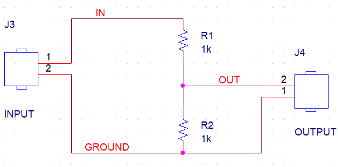
Before we start creating our PCB Layout based on this schematic design, we first need to make a few changes to the schematic. For any circuit that will ultimately be connected to another external circuit we must ensure there is a means of connecting the two circuits together. This is achieved by adding connectors or jacks. Let’s add the connectors as shown in .
To add the connectors use the Place>Part command (or the P shortcut), add the CONNECTOR library by navigating up one level in the root directory and then locate the CON2 part and place it twice, as shown in . These are the input and output headers. You may need to use right-click>Mirror Horizontally or Vertically or the right-click>Rotate command to get the orientation to match the schematic.
Change the name of the connector (by double clicking in CON2 text) to INPUT and OUTPUT in the Value field in the Display Properties box.
In complex circuits there can be very large numbers of nets. Nets can be given a name (an alias) and using aliases can make the design process much easier. To do this click Place>Net Alias (or use the N shortcut). In the Place Net Alias popup window, in the Alias field type IN and click OK. Click on the wire that is to form the IN net, as shown in . Press ESC to end the net alias placement process or the right-click>End Mode command. Repeat this process to assign the GROUND and OUTPUT net aliases to the wires, as shown in . Your circuit should now look like .
The schematic so far only includes component symbols that allow us to analyse the circuits functionality, however the design does not yet have any details on the actual physical dimensions and geometries for these components. Of course, in order to design the final PCB layout it is essential such information is included in the design. We will do this next.
To do this we assign each component with a footprint. Footprints depict the physical pin positions and sizes of the actual device. It is important the correct footprints are used otherwise the manufactured PCB may be incorrectly designed and may not be able to mount the desired component. Footprints are largely standardised for many components, but for more esoteric devices their footprints can also be downloaded directly from the component supplier or manufacturer. This can save designers a great deal of time.
For our design, we next need to assign the PCB footprint property values for all the parts in the design. You will need to specify the PCB Footprint property values for the names of the footprints that match the footprints in your libraries. Typically, in your Cadence folder, e.g.:
C:\Cadence\SPB\_17.4\share\pcb\pcb\_lib\symbolsyou will find the existent footprints for your designs. Please note that this folder path may change depending on the exact specifications and type of computer you are using.
Other than using standard footprints or importing new footprints directly from the manufacturers, it is also possible to create your own if required. Should you require a footprint that is non-standard and that has not been provided by the supplier, SnapEDA is a commonly used webpage from which you can download missing PCB footprints. In our present design we will be using footprints that have already been made available to use in the software. Footprints have the file extension .dra. Note that there will need to be an exact match between the numbered pins in the schematic part and the numbered pins on the PCB Footprint.
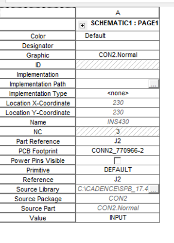
One possible method to add footprints to your schematic components is described in this section. Let us add a footprint for one of the connectors. Select the INPUT header and right-click>Edit Properties… to launch the Property Editor. (You can also double-click on the part to bring up the Property Editor). It is often easier to use the spreadsheet in the Property Editor window by transposing it. To do this double click in the top left cell. The value in the “PCB Footprint” field defines the file called for the parts footprint. Ensure that all the cells have the same content as shown in . When you are finished, save the changes (File > Save 💾) and close the Property Editor. Repeat the steps for the OUT header.
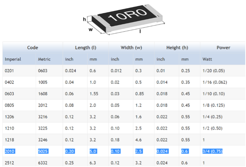
Now we can change the footprints used for our resistors. To do this we change the name of the file in the PCB Footprint cell for each of the resistors. Here we will make the footprint of R1 and R2 named smr2010. Once you have typed smr2010 into the correct cell in the Property Editor table, make sure to click the Apply button above the table to action the changes. In you can see the width, length, height and power associated with standardised resistor dimensions for different codes of Surface Mount Resistors (SMR).
Design Rule Checks
After you have completed your design, it is recommended that you undertake a Design Rule Check (DRC) which is used to help identify and fix any design errors. DRCs use design rules which define limits and tolerances on component spacing, trace dimensions and a variety of other physical design elements. DRCs can also check for functional errors such as non-connected pins and wires. It is essential that we regularly check for errors to ensure that they do not propagate through our design work. This is incredibly important for more complex projects as you will see in the second part of this unit.
To run a DRC:
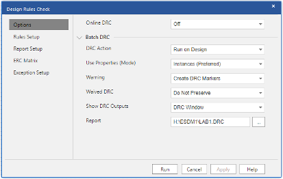
In the Design Rule Check dialog box change the Online DRC to off and specify any other our preferences. In our case the design is extremely simple and there is no need to adjust the other standard settings.
To run the DRC, click Run.
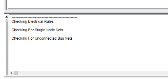
When the DRC has finished a DRC report is generated. This report will inform you of any errors in your design that will require your attention to fix. To view the DRC report you can either look at the Session log or access the report from the Outputs folder in the Project Window. You should get the results as shown in . Should your report have any errors these will be highlighted on your design. All errors will have a corresponding description that will provide some insight as to why there is a particular type of error at any given node as well as how to fix them. Ensure your design is error free before continuing with this script.
Creating a Netlist
The next step towards creating a real-world product is to create the PCB layout. PCB layouts can of course be drawn manually, though these are often prone to human error and cannot be automated. A more efficient use of time is to create a netlist that tells the software what nodes in the circuit are connected. A netlist can then be used to inform or automate the PCB layout design.
In our design so far we have manually wired up the components. Based on this correctly wired schematic simulations were executed to ensure that the circuit functions as our theory and analytical considerations would suggest. The next step is to create the PCB layout.
For a functional PCB layout, the layout designs require the correct wiring to be communicated from a schematic phase of the design to a physical wire and footprint layout phase of the design.
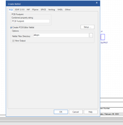
As shown in , to create a netlist for our design:
In the Project Manager window select the design file entry .\XXX.dsn.
Select all the components in the schematic, ensuring they are all highlighted pink. From the Tools menu select Create Netlist. The Create Netlist popup appears.
Click Yes if a popup asks you to create a new Netlist Directory. A progress bar should appear and execute.
Problems with PCB Editor Crashing – Potential Fixes
- Make sure all files are saved in the H: drive
- If they are not, then create a new blank project and copy and paste the design into this. Then, netlist etc.
- Ensure this is then the file you use.
- Make sure there are no spaces, numbers or special characters in your filenames and that the filenames are all lowercase.
- You can try making a completely new file, saved on H: drive. This can have a copied/pasted design.
If you are then still experiencing issues, one fix is to create the board file separately and sync this to your design. To do this:
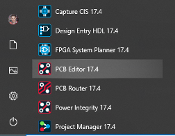
- Open PCB Editor from the task bar
- Make a .brd file (maybe draw a rectangle and save the file)
- Close PCB Editor
- Open Capture CIS
- Open your file, following all the rules previously mentioned
- Netlist
- Click PCB Design Sync
- In the window, click on the dots from Board, and select the .brd file you just created (see )
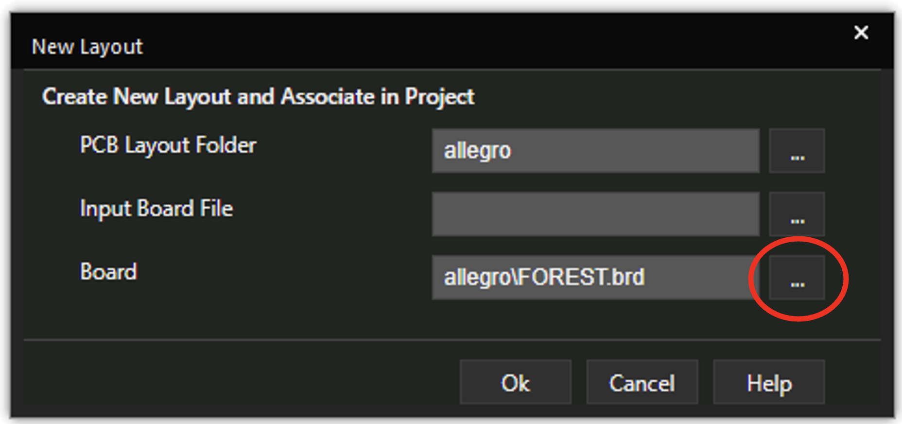
- Note, this is usually saved automatically in
C:/SPB_Data - This should open PCB Editor automatically and load the .brd file
- If it crashes, it is still worth checking: open the .brd file and click Place > Manually
If this has worked, then your components will be listed under Components by refdes.
Setting up PCB Editor
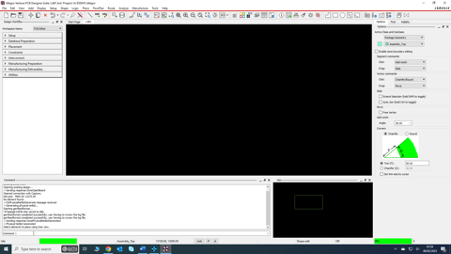
We can now start work on the physical design of the PCB layout, as shown in .
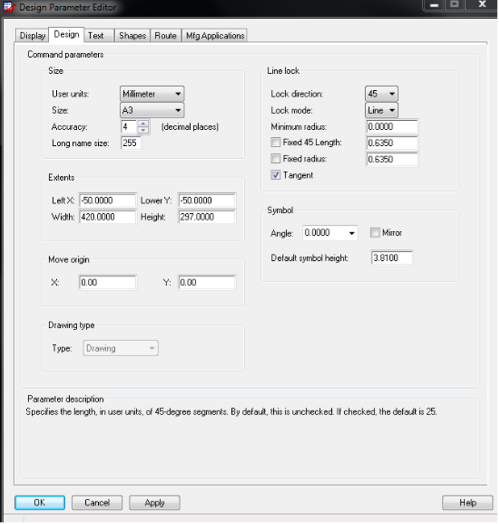
- Select Design Parameters.
- In the Design tab change the following settings:
- User units = millimeter
- Size = A3
- Left X and Lower Y = -50
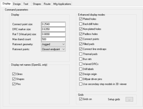
- In the Display tab enable the display settings by selecting the radio buttons as shown in in the Enhanced display modes section of the window.
- Click Apply and OK to save the settings.
The editor, by default, anchors components to a hidden grid within the design space. This can be frustrating as it can prevent you placing components in specific positions.
Creating a Board Outline
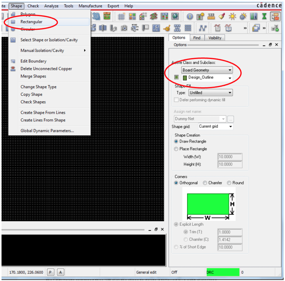
All PCBs have a finite extent, exterior to which components cannot be placed. This is defined by their edge. The board outline (or Design Outline) defines the boundary of the PCB. To create a board outline in PCB Editor follow the next steps.
- Click Shape>Rectangular (Although Polygon and Circle can also be used). See .
- Set the Options menu on the right-hand side as shown in , for Class and Subclass (layers in PCB Editor) make sure to select Board Geometry and Design_Outline. These properties ensure that the software knows what these geometries are.
In the command window at the bottom of the screen, type x 0 0 followed by the return button. This will start drawing the rectangular shape from the co-ordinate (0,0) in the design space.
In the command window type x 50 30 followed by a return to complete the rectangular shape at the co-ordinate (50,30).
Right-click > Done (or press F6) to end the active command. Use the
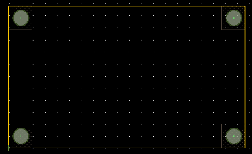
You have now drawn a PCB outline that is 50mm in the X and 30mm in the Y.
Changing Layout Colors
For complex designs consisting of hundreds of nets and thousands of components it is often convenient to use colours to help distinguish features within your design. To do this:
- Go to Setup > Colors menu on the left-hand side.
- Select Geometry and then choose a colour in the bottom of the pane then select the coloured swatch next to the subclass you wish to change (in this example choose Yellow and then choose the Design Outline). The swatch colour should then change to the colour selected. Any changes are made dynamically, and your design outline will change to Yellow in this case.
- Click OK to close the Colour Dialog.
Adding Mounting Holes
All PCBs must be mechanically mounted to or within an enclosure to ensure they do not move during their use. Often this is achieved using screws or bolts. This requires us to integrate mounting holes into our PCB design which will be manufactured at the same time as the other elements on the board. To add mounting holes to the PCB:
- Click Place > Manually.
- Since we want to place 4 mounting holes we must place 4 symbols. Select the Advanced Settings tab. Change the AutoNext from Enabled to Disable. In the List construction field tick the Library box and the Database box. On the Placement List tab in the Components by refdes dropdown menu select Mechanical symbols and choose MTG125.
- Left-click on Hide
The Placement dialog closes and the mechanical symbol MTG125 is attached to the cursor ready to be placed on the design as many times as you wish. You can either left-click to place the hole at the required location or type the x/y co-ordinates in the command line to place the tooling hole at the required location. For this example we will enter the co-ordinates directly.
- Place the next three symbols at x 2.5 27.5, x 47.5 27.5 and x 47.5 2.5.
- Right-click > Done (or use the F6 shortcut) to end the mechanical symbol placement.
- File > Save 💾 to save your board design.
Your PCB layout should look similar to that shown in .
Placing Components
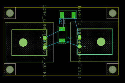
In this section we will use manual placement to create the PCB for the schematic we created earlier in the lab. There are different ways in which you can select a component for placement. In this tutorial you will learn to place components by refdes only.
From the Place menu select Manually.
Select the J1 component by clicking the check box next to the component name.
Left-click Hide. The Placement dialog box closes and the component (in this case J1) that you have chosen is attached to the cursor.
Move the component to the desired location where you would like it to be positioned. You can use right-click > Rotate to rotate in either direction and at any angle set by the Options fold out menu Rotation angle setting. Repeat this placement process for all of the raining components. Note that as you place each component it is removed from the placement list. You should now have your four components and board layout as depicted in .
Design Rule Checking
Regular design checking is essential to ensure a functional and manufacturable designs in both the schematic and layout phases of a design. Let us then run a DRC on the layout design we have just created.
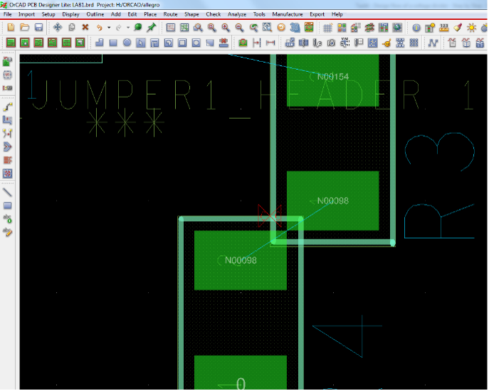
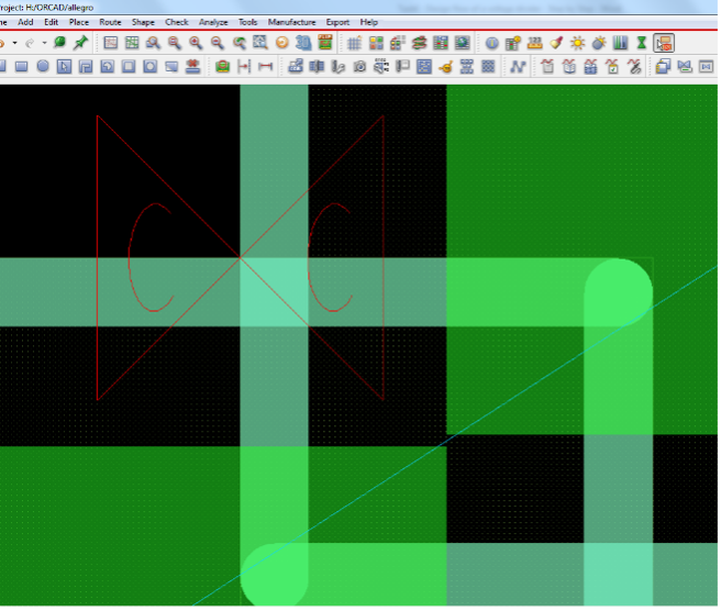
PCB Designer Suite allows you to run DRC online (On) or in batch mode (Off). For our simple design we will turn the Enable On-Line DRC to off as there is no need for the additional online resources for such a small design. To do this, click on the Setup tab and click on the Enable On-Line DRC. Part of the DRC program runs silently in the background, and while placing the components, if there are any design rule violations, then error markers are displayed on the board. An example of a Placement DRC (C-C) is shown in red in and magnified in . Ensure your design is error free before progressing to the next section.
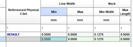
Setting the Design Constraints
Design Constraints refer to the limitations of the manufacturing process. Not all geometries can be produced. To set these up:
To configure the basic spacing and physical constraints for your board design, from the top ribbon select Setup > Constraints > Physical.
On the right you will see a spreadsheet that states all of the present default physical constraints, such as line width, necks, and so on.
Routing
Routing is the process of laying conductive tracks / traces down onto our PCB to electronically connect our components together.
After completing the board placement, you can route your board to complete the electrical connections between components. PCB Designer Suite supports both manual routing and auto-routing. For complex boards, with many thousands of components, it is generally good practice to first route any critical nets manually, lock them and then autoroute the rest of the board but this is user specific and may depend on the design you are working on. A detailed understanding of the mathematical algorithms behind auto routing is beyond the scope of this unit.
Manual Routing
The general steps involved in the manual routing process are:
- Check the board outline, via definitions, routing and via grids. (Note: A via is a metal plated through hole that electrically connects two conducting layers in a PCB).
- Route power and ground.
- Fan out any surface mounted devices and verify their connections to power and ground.
- Route the remaining tracks using the manual routing tools.
- Optimise routing using the manual routing commands.
- Check for route spacing violations and check routing statistics.
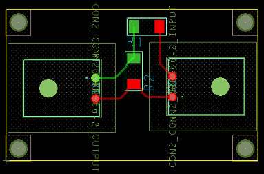
shows and example of a the manually routed IN, OUT and GND nets for our design. To do this:
Select the Assign Colors > command (Display > Assign Color) and pick a colour from the Options menu. Choose red here.
No further guidance.
Left-click the More… button next to the Find by Name dialog box and a list of all of the available nets appears. In this case this is all our nets (Ground, In and Out).
No further guidance.
All the wires in the originally blue rats nest associated with the IN and GROUND nets are now coloured red in the design. This is useful in ensuring we wire the design up correctly. We can now wire up (route) the design manually using the colored rats nest to guide us.
No further guidance.
Repeat the above steps for the remaining nets. You circuit should now look like .
Adding Vias and Layers Whilst Routing
Vias and layers allow us to create more complicated designs consisting of more layers of copper within our PCBs. Vias are connecting wire or pins that connect different layers within a PCB. No vias are required in the present design and the below is for your reference. To add a via;
- Left-click on the net to be routed.
- Route to a point where you want to add a via, right-click on the net and select Add Via (or double-click the left mouse button). A via is added. The current Active layer becomes the Alternative layer and vice versa. For example, if you have a Top and a Bottom layer, where Top is the current Active Layer, then when you add a Via the Bottom layer will become the Active layer and the Top layer becomes the Alternate layer.
- Draw the net through the desired path.
- When you have completed routing, right-click on the net and select Done.
We will not use this option as it is not required due to the simplicity of our circuit. However, you may require this in Part 2 of the unit.
Checking & Reviewing
Our design is nearing completion. As good engineers we need to check and review our work. There are many ways to review your design once our initial design efforts have been completed. A quick design check is to ensure that all the components are placed and routed correctly to ensure the circuit will function as intended.
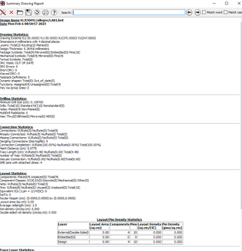
It is possible to run a variety of checking reports giving information about your design. To do this click Tools > Quick Reports > Summary Drawing Report. A summary of your design is produced in a popup window, as shown in .
Back Annotation (*optional)
While creating a PCB, you might make some changes in the PCB board (.brd) file. As a result, the board file and the design file in Capture may be out of sync. To ensure that both these files are in sync, you can back annotate the changes in the PCB file to OrCAD Capture.
When you back annotate, information, such as pin and function swaps and component names (changed due to renaming) gets added on to the schematic in OrCAD Capture.
To back annotate changes;
- Open the XXX.opj in Allegro Design Entry CIS where we built the schematic model.
- In the Project Manager window, select XXX.dsn.
- From the Tools menu, select Back Annotate. The Back annotate dialog box appears.
- Select the Generate Feedback Files option.
- Left-click OK in the back annotate dialog box. A message appears asking you to save your modified design prior to creating a new netlist file and a .SWP file.
- Click Yes