PCB Circuit Simulation in OrCAD
Designing PCBs in OrCAD Version 17.4.
In Part 1 of the unit you will:
- Become familiar with OrCAD and the design flow process
- Simulate a simple circuit
- Design the physical layout of a simple circuit
- Generate gerber and drill files for this design
As with most designs, to prepare for the detailed circuit layout design, it is first convenient to design the circuit schematic, understand its operation and conduct simulations, and then translate this schematic into an equivalent circuit or physical layout. This manual, written for OrCAD vs 17.4, covers this entire process with a particular focus on the design flow of a simple potential divider circuit.
Introduction
The Cadence OrCAD PCB Designer suite comprises three main applications.
Captureis used to draw the schematic circuit on the screen (schematic capture). A netlist, which describes the components and their interconnections, can then be generated and subsequently linked to a simulation tool (PSpice) and PCB design editor (Allegro).PSpicesimulates the function of the schematic circuit designed in Capture. PSpice is not the focus of this unit. PCB Editor is. Nevertheless, PSpice does remain an important part of the design process and is required to holistically introduce the design layout process in its entirety.Allegro(PCB Editor) is the application within which a printed circuit board (PCB) is designed. The output from PCB Editor is a set of files that can be sent for production to a PCB manufacturer.
For laying out a PCB you will need footprints or package symbols. Footprints show the physical size and shape of the pads and the outline of the package (e.g. resistors, capacitors, op-amps, diodes, etc.). They are used to layout the circuit in PCB Editor. These are stored in different sets of libraries and you must select the files needed for a particular design.
Design rules are required to layout the circuit on the PCB in such a way that the design is likely to be manufacturable. There are many design rules relating to various elements of a design. Only the basic rules will be considered here. These specify the minimum width of tracks and the gap between them. Manufacturers often express these rules as meaning minimum widths of 10 for tracks and 8 for gaps. The units are typically in mils, an imperial measurement where 1 mil = $\frac{1}{1000}$ of an inch. Further design rules control a diverse range of features, such as the spacing between tracks and pads, whether vias are permitted and the impedance of tracks. The following content will guide your through the design of PCB based on a simple potential divider.
Simulation in Capture CIS
Create a Project
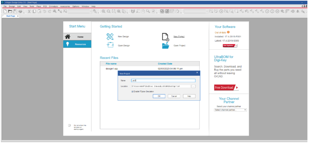
Open Capture CIS 17.4 in the Cadence PCB 17.4-2019 start folder. The Allegro Design Entry CIS start page will appear.
E.g., whether it is saved in your H: drive or in your local C: drive (of the PC you are using during this session) as this will impact your ability to return to the project at a later date. For safety you are also advised to regularly back up your files to a destination of your choosing. You are encouraged to save your project to your networked H: drive as this will allow you to access the project on campus and via Uniapps.
Adding the Libraries
Before we can commence our design, we first need to start by adding the Libraries that contains details on the components we will use. To do this, select the SCHEMATIC1 : Page1 tab to open the schematic page. Click Place>Part from the menu and a the Place Part menu should appear on the right-hand side of the screen. Next use the Add Library icon to add the required libraries as depicted in .
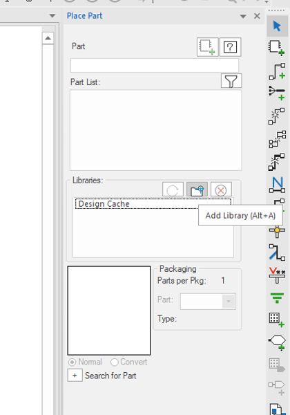
…\SPB\_17.4\tools\capture\library\pspicefor the PSpice libraries. Click Open to add the libraries. The Part List: and Libraries: fields in the Place Parts menu should now be populated.
Placing & Wiring Components
- The exact positioning of the schematic components is not important to having a working example, but please correctly place the various elements as in as it will be easier to debug the schematic and get the circuit simulating as expected if the design has similar positions to that shown.
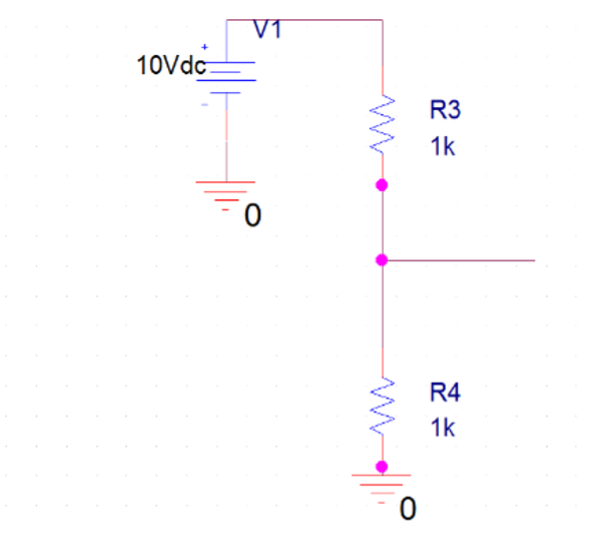
- Once the libraries have been added, place a resistor, R from the Analog library. Type R in the Part edit box and press enter to get the R graphical part on the mouse cursor. Use right-click>Rotate, or press the R key on the keyboard, to rotate the R, so that the resistor is vertical then left-click the mouse to place the R part towards the upper left of the page. Right-click>End Mode, or press the Esc key, to end the placing process. Repeat this process to place a second resistor.
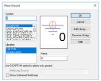
Next, we need to place a DC voltage source, VDC. To do this, click Place > PSpice Component … > Source > Voltage Source > DC. Set the DC voltage source to 10V by clicking on the “0Vdc” and right clicking > edit properties. In the Value field type “10Vdc” and click OK. Use the same approach to set the values of both resistors to 1K. The two grounds can be placed directly from the Place tab () or by using the G shortcut on the keyboard. Place all the components shown in to complete the circuit.
Next, these components must be wired together, as shown in . Do this using the wire connection tool in the Place tab or using the W shortcut. When wiring up the circuit make sure to click on the component square terminations. To end a floating wire, simply right-click and select End wire or use the Esc shortcut. Once connected your schematic should look like .
We can now start to explore how this circuit operates.
Circuit Operation
We can assess the functionality of the circuit in many ways. Here we will simply measure the voltages at various nodes within the circuit. We can do this using a voltage marker to observe the voltage, for example at the output of the voltage divider. A voltage marker is illustrated in green in .
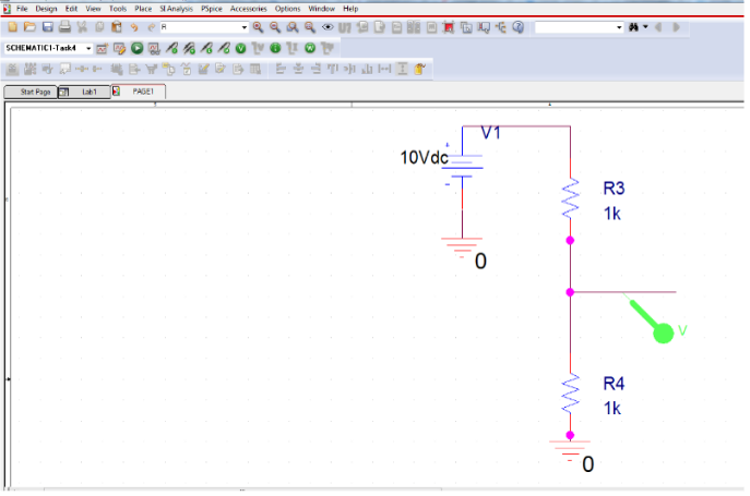
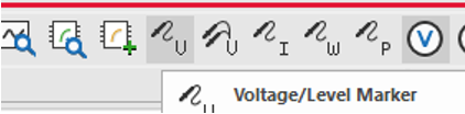
This voltage node simply tells the program at what point in the circuit the voltage is measured and not what is measured. Place a voltage marker as shown in using the Voltage/Level Marker icon, as shown in . To give the app all the required details we first need to create a New Simulation Profile which can be found in the PSpice tab () where we can create a “New Simulation Profile”. In the New Simulation pop up window, set the Name field to “Simulation” and click OK.
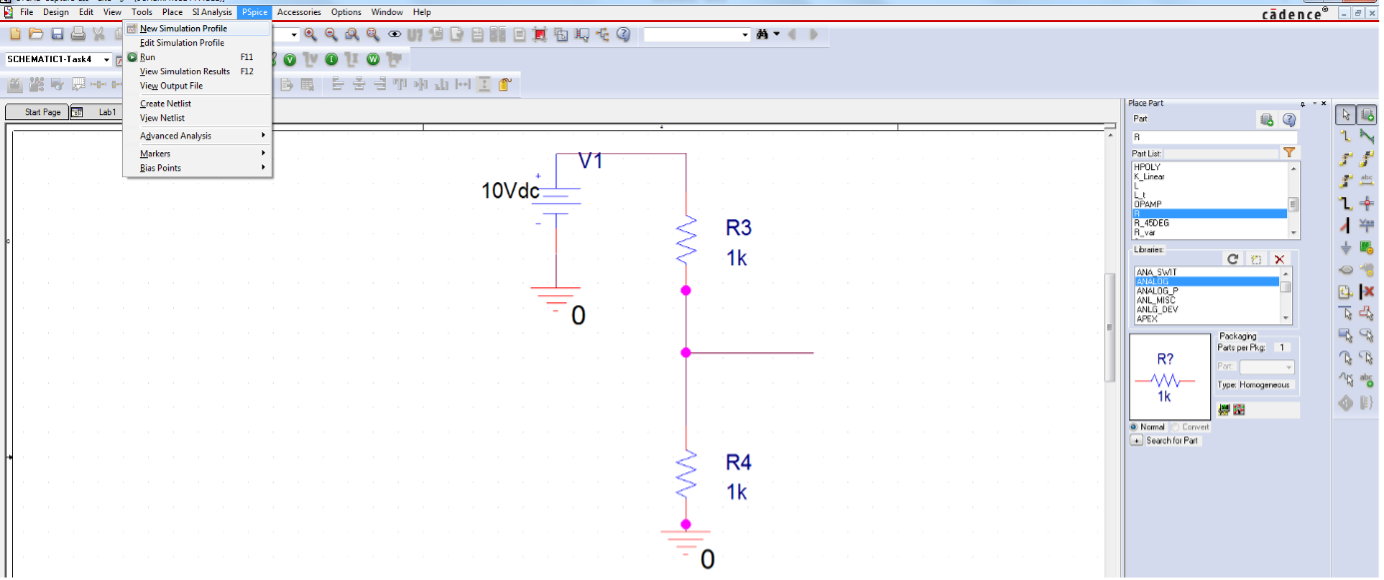
We can now setup the analysis in the Simulation Settings pop-up window. The simulation run sequence involves setting the Simulation Profile for the required simulation type and then running the simulation. The Simulation Profile can either be edited for each simulation, or a New Simulation Profile can be created, as required. The small advantage to having multiple Simulation Profiles is that it will then be possible to switch between the simulation settings without editing the Simulation Profile. This allows for rapid testing and simulation work. There are four basic Analysis Types for PSpice:
- Time Domain (Transient)
- DC Sweep
- AC Sweep
- Bias Point
The Bias Point simulation activates any DC sources within the circuit and allows the circuit to achieve a stable state. The other simulation types will start by running the Bias Point simulation, to get the circuit to a stable state, and then run the selected simulation type immediately after this. A DC Sweep will apply a range of DC values to a Voltage, or Current, source, a Model Parameter, a Global Parameter, or Temperature. An AC Sweep will apply multiple AC values to any AC sources within the design. AC sweeps are typically used to evaluate the frequency response of a circuit. A Transient analysis will evaluate a circuit in real time such that it is possible to view the waveforms within the circuit. A transient analysis will give results that are very similar to what you would observe if you were repeating the analysis in reality on a real circuit using a bench top oscilloscope. In the Analysis Type: drop down menu, select Time Domain (Transient). We can now set up the various features of the analysis.
Transient Simulation
In this section we will run a transient analysis for our circuit and will view the output waveform. We can also check for correctness using simple calculations learnt in other units.
First, we need to create the simulation profile. With the Simulation Settings – Bias window still configure the Simulation Profile parameters as shown in . Based on the settings we added, this simulation profile will run the simulation for 1ms (1000ns). Do not worry about the other settings for the moment. Click OK on the Simulation Settings pop-up window.
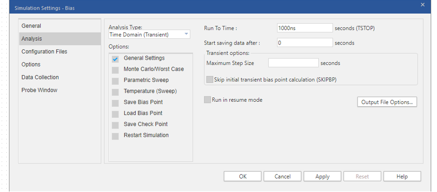
Transient Profile
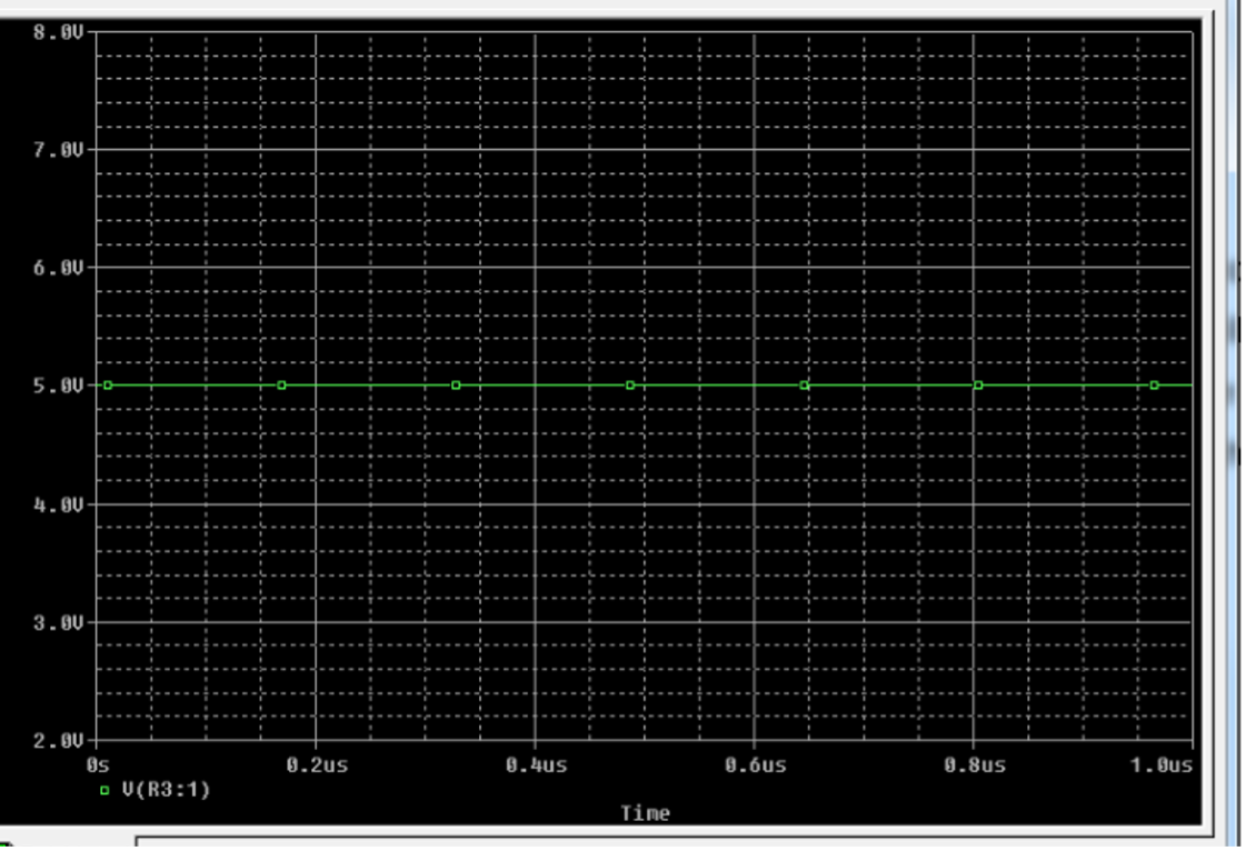
We can now run the simulation. To do this click PSpice>Run from the main ribbon at the top of the graphical user interface (GUI) or use the F11 shortcut. The simulation will run and a Probe Window (Allegro PSpice Simulator) will open showing the waveform with a graph of voltage against time. You will see a straight line across the voltage output of your voltage divider. The output should look like .
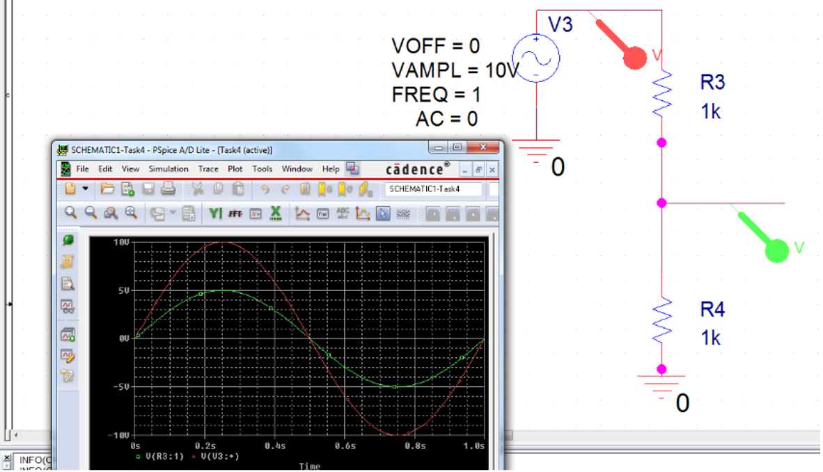
Let’s now adjust our circuit to make better use of the transient analysis function. To do this change the power source to an AC voltage source that will apply an alternating bias across our divider. To do this, type VSIN in the Part field in the Place Part menu. Place the VSIN component on the design sheet. Delete the DC voltage source and wire in the new AC source.
To explore how the circuit operates when excited with an AC source lets add another probe on the positive voltage side of the new AC voltage source. This will allow us to simultaneously view on a single plot, the initial AC voltage and the AC voltage at the first voltage probe we placed. For clarity, the two voltage probes should now be located as shown in . To ensure that our transient simulation runs for a sufficient time so that we can observe the AC time dependency of these voltage probes, next edit the simulator profile to have a run time of 10 seconds.
We have now created a schematic of our circuit and have a good feeling for how the circuit operates. The next step in the design of this circuit is to think about how we go about manufacturing it. To do this we need to consider the physical layout of the circuit.