Op-amp Interface Circuit Design
Introduction
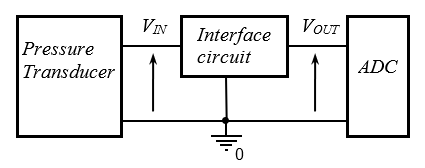
This exercise involves choosing and proving the design of an interface circuit to scale and level-shift a pressure transducer signal, so that it better matches the input voltage range of an ADC (analog-to-digital converter) and may be more easily and accurately read by the data acquisition electronics of a computer. It is hope you will be able to quickly test your finalised circuit by simulation before checking operation by experiment.
Equipment
Collect the following equipement for this experiment:
- Circuit breadboard and box of connecting wires;
- Resistors 10k $\Omega$, and 22k $\Omega$ may be provided other values available from stores;
- 8-pin op-amp integrated circuit; extras available from stores.
- OrCAD/PSPICE circuit-simulation software package using transient analysis simulations.
Design specification
Design an op-amp circuit by adding to the configurations in to interface a pressure transducer output to a computer ADC (analogue-to-digital converter) input. The ADC input voltage range is 0V and 5V while the pressure transducer output range is between -250mV and 250mV. Design the interface circuit to make full use of the ADC input voltage range. Only +10V and –10V power supplies are available to energise the circuit.
Exercise 1
Sketch a graph of output voltage $V_{\text{out}}$ (vertical axis) versus input voltage $V_{\text{in}}$ (horizontal axis), mark the input and output voltage value limits on it, sketch a line to show the variation alignment. By noting the linear form of the graph, derive an equation which expresses output voltage as a function of input voltage.
$V_{\text{out}} = \qquad V$
Briefly explain what the interface circuit must do to make full use of the ADC input voltage dynamic range.
Interface circuit suggestions
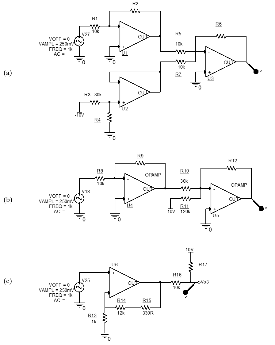
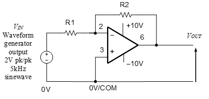
If you do not have a good alternative design, one of the following three designs may be used. Some resistor values have been omitted which you must size in order to use them. The earlier, easier-to-understanding cir-cuits have more resistor-value omissions. There is a cost advantage in minimising the number of op-amps you use, and it simplifies experimental validation. Use an earlier design if you cannot get correct operation with the final design. The 0 to 5V output you are aiming to obtain in response to a $\pm 250mV$ input is illustrated in .
Testing the interface circuit design by simulation
Quickly enter your circuit into the Cadence/OrCAD PSPICE circuit simulator and run some tests to confirm that you have correctly sized resistor.
Exercise 3
List three ways in which you carefully checked that your circuit really does work and accurately meets the specification, other than just glancing at the scope and assuming the output is good.

Testing your circuit experimentally
Exercise 4
Obtain the required resistors from stores and using a prototyping breadboard, and the smallest possible number of wires without a lot of daisy-chaining, build you circuit. Use the power supply connection method described below. Test your circuit with the waveform generator output set to a $\pm 250mV$ sinewave in high-Z mode. Display the input and output of the circuit as shown in and download the display to a flash memory drive or take a photo using a smart phone.
If you complete the lab early, test whether the circuit works accurately at high frequency. How could it be improved if the high-frequency precision is found to deteriorate.
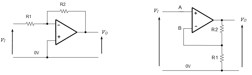
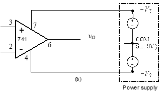
You may wish to use one or more of the inverting or non-inverting amplifier configurations shown in as part of a circuit to implement your mathematical equation. Please note that, although the op amps will require +10V and -10V power supply connections as shown in , and when you experimentally check your circuit design, these are usually not shown on circuit schematics drawn to show the signal processing functionality. You may skip the connection details below until you are ready to connect your finalised op amp circuit, tested by simulation.
Use the breadboard and wire links provided to first connect the op-amp circuit shown in and to energise the op amp and then add the resistors as shown in below to set the overall gain of the inverting amplifier stage. How to do this is explained in more detail below.
With the power-supply switched off, connect the 0V, +ve and –ve power-supply outputs first to the 4 mm terminal posts on the breadboard, and then connect these to the op-amp as shown in Fig.2b using short, tidy links.
Connect the red of one twin lead with 4mm plugs to the +25V power supply output terminal and the black of the same lead to the -25V power supply terminal. Red and black posts on the breadboard should be matched with red and black power supply terminals.
Double up the 4mm connectors on another twin wire lead and connect to 0V/COM connection on the power supply to a separate post on the breadboard, for example green. Connect the waveform generator output to the 4mm posts to supply a variable level sinewave to the amplifier configuration. Make sure that the 0V of the waveform generator and the COM (or 0V) output of the $\pm V_S$ supplies are connected together as shown in .
Now connect the bottom of all the breadboard posts and any resistors, such as R1 and R2, directly to the amplifier using as few daisy-chained wire links as possible to complete your circuit design.
Turn on the Agilent power supply and enable its output. Select +25V to monitor the voltage set on the +25V output and increase the voltage to 10 V. Press and hold the Tracking key on the power supply for a count of five, so that the –25V output level follows, i.e., tracks, the +25V output setting.
Select –25V to display the voltage set on the -25V and check that the voltage is now –10 V. The op-amp should be drawing very little current and not getting hot.
Set the waveform generator to give a 500mV pk/pk, 1kHz sinewave output. Connect the two oscilloscope probes – both crocodile clips to 0V and the probes tips to VIN and VOUT – to display the input and output sin-ewaves on the oscilloscope. Turn the oscilloscope on and press Autoscale. If a waveform is not displayed, check the waveform generator Output is enabled and probe crocodile clips are both at 0V and probe tips are connected to the signals.
Exercise 5
If you finish early implementing a 2 or 3 op-amp design, then complete the single op-amp design. If you complete that, assist other groups who are struggling.
Reflection on skills and learning
Complete outside the lab if you run out of time in your lab notebook. Comment on your individual attainment as suggested below.
What percentage of the lab work did you complete? How do you rate your participation as a lab group member?
What level of proficiency do you feel you achieved in designing a practical interface circuit and testing, debugging, and making measurement on a circuit simulation or practical circuit. Choose one of the following and add a comment.
- High –now confident in completing an interface design using one or more standard op-amp configura-tions and then testing and debugging by simulation or experiment. Can envisage using in —- application?
- Medium – some further practice required but have reasonable understanding of the design, test and debug processes required to validate a design. More practise especially required in —–?
- Basic – can follow the process and results but need significantly greater individual practice in some of the design and validation stages. The main obstacles to to more confident design and simulation or experimental validation are —–?
List two or more ways in which attending and completing the lab work has been of value.
List any suggested changes to the lab work that you identified which would facilitate circuit theory learning and acquiring circuit design and validation skills.