Characteristics of Coupled Transmission Lines
Introduction
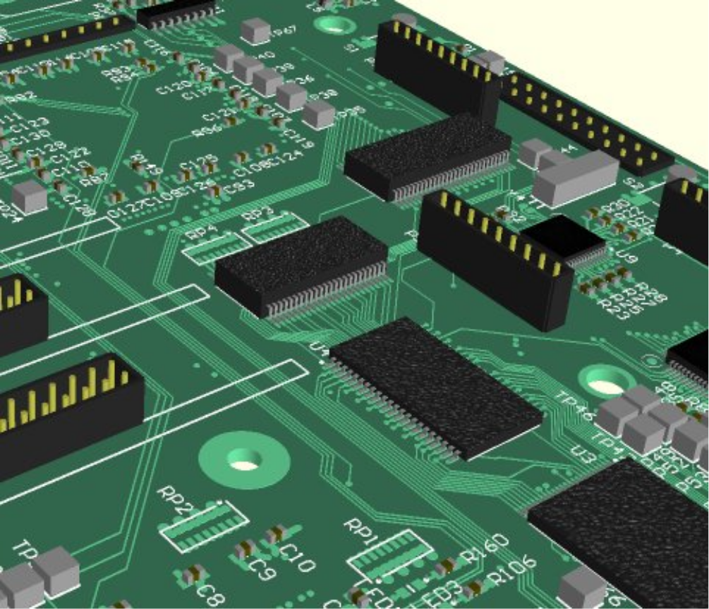
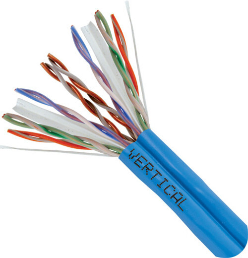
The aim of this experiment is to investigate and characterise coupling between parallel circuits. These are frequently found on circuit boards as shown in . In cable harnesses, cable wiring looms or ‘bundles’ such as multiple telephone and ethernet connections in trunking, as illustrated in there can be many parallel wires carrying multiple signals. Coupling between these tracks or wires can cause signals to ‘leak’ between circuits that might be thought to be independent.
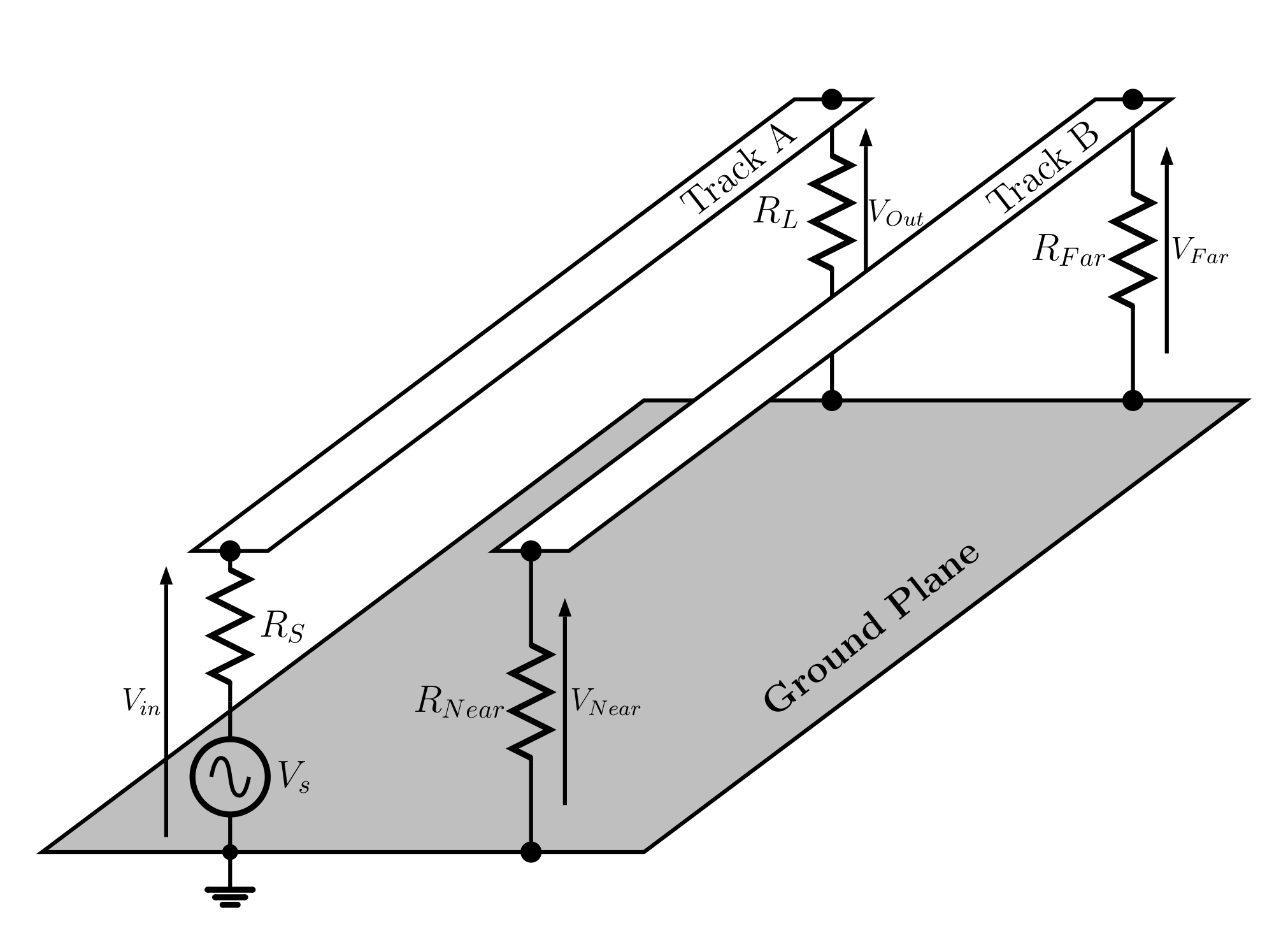
Two parallel tracks are illustrated in . Track A connects a source to a load. Track B runs close to Track A and some signal can couple across and appear at the Far end and at the Near end. The voltage transmission to the load is $T_{OI} \,=\, V_{Out}/V_{in}$, the voltage transmission to the Far end is $T_{FI} \,=\, V_{Far}/V_{in}$ and the voltage transmission to the Near end is $T_{NI} \,=\, V_{Near}/V_{in}$.
In this experiment consideration of the CMOS decision voltage levels helps to illustrate the importance of how coupled lines can be used. CMOS logic circuits powered between $V_{CC}$ and $V_{SS}$ see signals between $V_{SS}$ and $0.3\times V_{CC}$ as logic zero, and between $0.7\times V_{CC}$ and $V_{CC}$ as logic one. When powered between $V_{CC}=3.3V$ and $V_{SS} = 0V$ logic zero is between $0\,V$ and $1\,V$ while logic one is from $2.3\,V$ to $3.3\,V$. Circuit damage can result from inputs at $V_{CC} + 0.5\,V = 3.8\,V$ and at $V_{SS} - 0.5\,V = -0.5\,V$. In the waveforms seen note where signal logic levels could be confused or perhaps cause damage. It often helps to scale the voltage source amplitude so that the input pulse amplitude is $3.3\,V$ to examine the case where a logic one signal is applied.
Equipment
Personal computer or laptop with LTspice installed, and perhaps MatLab or Excel.
Preparatory calculations
-
Calculate the characteristic impedance and delay expected along a 40 section line with $L_0 = 47\,\mu H$ and $C_0 = 1.2\,nF$.
-
Calculate the reflection coefficient, transmission coefficients and return loss for load resistances $R_L=2\,k\Omega$, $R_L=385\,\Omega$, $R_L=165\,\Omega$, $R_L=20\,\Omega$, $R_L=2\,m\Omega$ (almost short circuit) and $R_L=200\,M\Omega$ (almost open circuit) on a line with the characteristic impedance evaluated in preparatory calculation 1.
Experiment
The coupled lines tend to involve capacitance, and perhaps inductance. Here inductive and capacitive loads are examined on a single line to illustrate their different ‘signatures’ when measuring on transmission lines.
Inductive and Capacitive Loads
-
In LTspice select File and Open to open the LTspice file EE22005_Transmission_Line_Load_L.asc
-
Select Simulate and then Run/Pause, or select the green triangle Run, to run the simulation. Then to monitor the input signal hover the cursor over the circuit at Rsource/in node so the red ‘probe’ symbol appears and select this by pressing the left mouse button. The input waveform V(in) shows two pulses with some ‘ringing’ at the leading and falling edges of the pulses and with a distinct decay with time during the pulse. This sharp edge and exponential decay is the time signature of an inductive load. Note the time delay between the incident pulse at the source and the pulse at the load, and compare with the delay for the whole line.
-
In LTspice select File and Open to open the LTspice file EE22005_Transmission_Line_Load_C.asc
-
Select Simulate and then Run/Pause, or select the green triangle Run, to run the simulation. Then to monitor the input signal hover the cursor over the circuit at Rsource/in node so the red ‘probe’ symbol appears and select this by pressing the left mouse button. The input waveform V(in) shows two pulses with some ‘ringing’ at the leading and falling edges of the pulses and with a distinct rise with time during the pulse. This exponential rise is the time signature of a capacitive load where the capacitance takes a finite time to charge up. Note the time delay between the incident pulse at the source and the pulse at the load, and compare with the delay for the whole line.
Time Domain Reflectometer or Line Tester
Examining the time response of a transmission line is often used to identify faults on a line. This is often done on power transmission lines and on telecommunications, broadband or telephone wire connections. The basic operating principle of the Time Domain Reflectometer or Line tester is examined here, and this also illustrates the basic measurement principle of a Radar system.
-
In LTspice select File and Open to open the LTspice file EE22005_Transmission_Line.asc
-
Select Simulate and then Run/Pause, or select the green triangle Run, to run the simulation. Then to monitor the input signal hover the cursor over the circuit at Rsource/in node so the red ‘probe’ symbol appears and select this by pressing the left mouse button. Also set a monitor for the load voltage. Note the time delay between the incident pulse at the source and the pulse at the load, and compare with the delay for the whole line.
-
To simulate a broken line fault in the transmission line select the Delete tool (black circle with a white cross) and the delete inductor L37 by placing the cursor over it, which should now appear as a pair of scissors or cut icon, and select L37. Run the simulation and note the time delay between the incident and reflected pulses at the source.
-
Then reinstate L37 by pressing Ctrl-Z or using the Undo tool towards the top right of the toolbar. Then select the delete tool and delete inductor L32. Run the simulation and note the time delay between the incident and reflected pulses at the source.
-
Then reinstate L32 by pressing Ctrl-Z or using the Undo tool towards the top right of the toolbar. Then select the delete tool and delete inductor L26. Run the simulation and note the time delay between the incident and reflected pulses at the source.
-
Then reinstate L26 by pressing Ctrl-Z or using the Undo tool towards the top right of the toolbar. Then select the delete tool and delete inductor L21. Run the simulation and note the time delay between the incident and reflected pulses at the source.
-
Then reinstate L21 by pressing Ctrl-Z or using the Undo tool towards the top right of the toolbar. To simulate a short-to-ground fault as opposed to the open circuit faults examined in the last tests select the Ground tool and add a ground connection at inductor L35. Run the simulation and note the time delay between the incident and reflected pulses at the source and the amplitudes of the pulses.
The previous steps show how a Time Domain Reflectometer or Line/Cable Tester can be used to determine the delay time to a fault, and position if the propagation velocity is known. It also shows the type of fault in a line. These measurements also show the basic principle of operation for a radar system, identifying the time and therefore distance to a target. The reflection also shows how large the target is and gives some information on the type of target found.
Coupled lines
Parallel circuit tracks and cables in close proximity become coupled. In its most basic form there is a capacitance per unit length, $C_{c0}$ between the tracks, as illustrated in
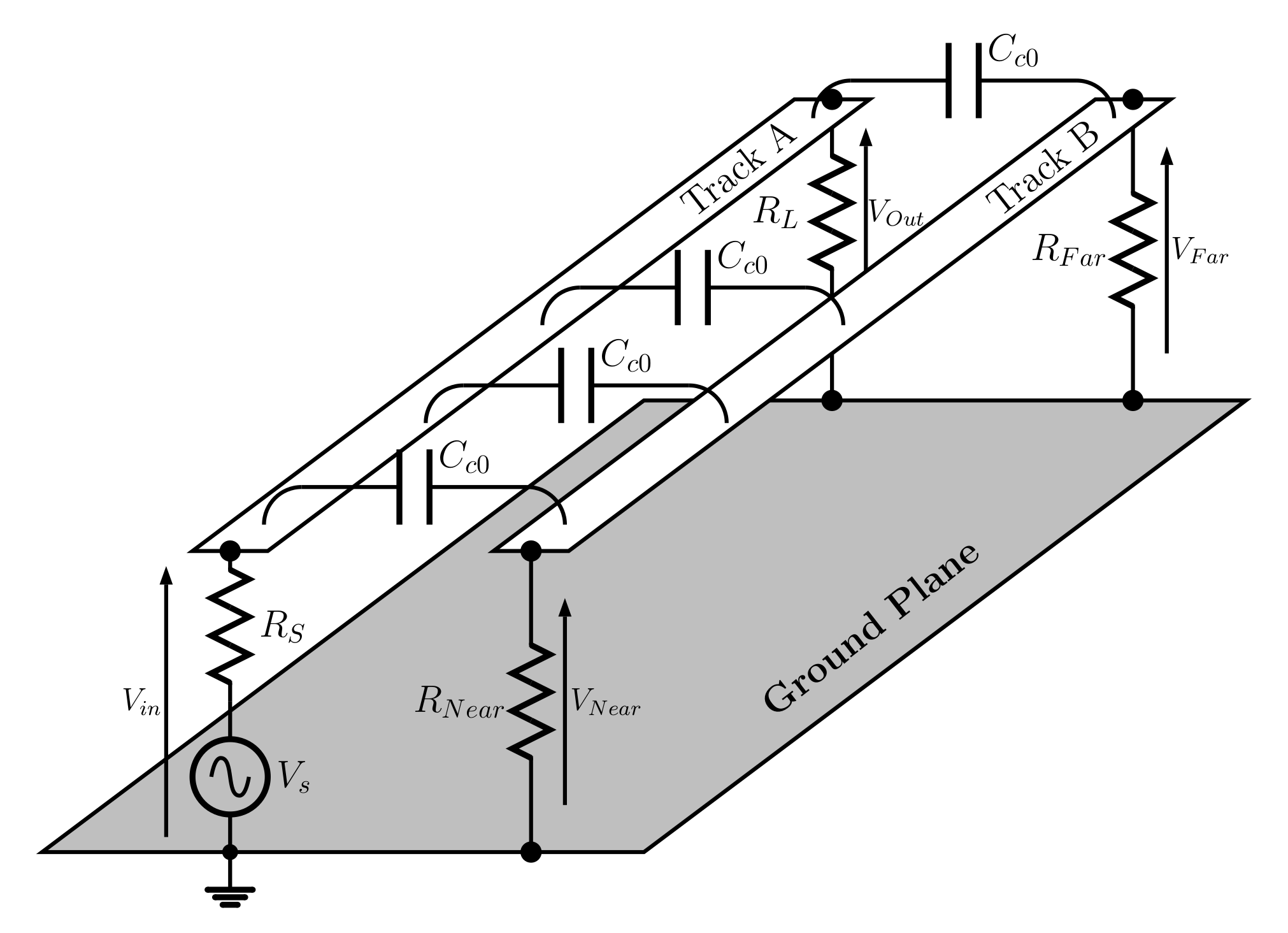
In this experiment the distributed coupling is simplified to five capacitances.
-
In LTspice select File and Open to open the LTspice file EE22005_Transmission_Line_Load_Cpl.asc. Check that the circuit has $R_S = R_L = R_{Far} = R_{Near} = 200\,\Omega$.
-
Select Simulate and then Run/Pause, or select the green triangle Run, to run the simulation. Then to monitor the input signal hover the cursor over the circuit at Rsource/in node so the red ‘probe’ symbol appears and select this by pressing the left mouse button. Also monitor the signals at the load, at the ‘Far’ load and at the ‘Near’ load.
Gradually increase, say in $0.25\,nF$ steps, the coupling capacitance per unit length, $C_{c0}$, from $0.25\,nF$ to $1\,nF$ noting how the responses seen at the Load, Far and Near outputs changes.
-
With $C_{c0} = 1\,nF$ note $V_{in}(t)$, $V_{Out}(t)$, $V_{Far}(t)$, $V_{Near}(t)$, $T_{OI}(f)$, $T_{FI}(f)$ and $T_{NI}(f)$.
-
With $C_{c0} = 1\,nF$ and $R_S = R_L = R_{Far} = R_{Near} = 2000\,\Omega$ set $V_S$ set such that the input pulse at $V_{in}$ is about the CMOS one level of $3.3\,V$. The voltage amplitude of the source can be set by right clicking on the pulse generator symbol and then altering $Von(V)$. Then note $V_{in}(t)$, $V_{Out}(t)$, $V_{Far}(t)$, $V_{Near}(t)$, $T_{OI}(f)$, $T_{FI}(f)$ and $T_{NI}(f)$.
Note where the CMOS voltage levels for logic states one, zero and undecided are met at the three outputs.
-
With $C_{c0} = 1\,nF$ and $R_S = 20\,\Omega$ and $R_L = R_{Far} = R_{Near} = 2000\,\Omega$ set $V_S$ set such that the input pulse at $V_{in}$ is about the CMOS one level of $3.3\,V$. Then note $V_{in}(t)$, $V_{Out}(t)$, $V_{Far}(t)$, $V_{Near}(t)$, $T_{OI}(f)$, $T_{FI}(f)$ and $T_{NI}(f)$.
Note where the CMOS voltage levels for logic states one, zero and undecided are met at the three outputs.
-
With $C_{c0} = 1\,nF$ and $R_S$, $R_L$, $R_{Far}$ and $R_{Near}$ set to produce a return loss of $10\,dB$ set $V_S$ set such that the input pulse at $V_{in}$ is about the CMOS one level of $3.3\,V$. Then note $V_{in}(t)$, $V_{Out}(t)$, $V_{Far}(t)$, $V_{Near}(t)$, $T_{OI}(f)$, $T_{FI}(f)$ and $T_{NI}(f)$.
Note where the CMOS voltage levels for logic states one, zero and undecided are met at the three outputs.
-
With $C_{c0} = 1\,nF$ and $R_S$, $R_L$, $R_{Far}$ and $R_{Near}$ set to produce a return loss of $10\,dB$ set $V_S$ set such that the input pulse at $V_{in}$ is about the CMOS one level of $3.3\,V$. Then add an open circuit and/or short circuit fault at inductor L32 on Track B. Then note $V_{in}(t)$, $V_{Out}(t)$, $V_{Far}(t)$, $V_{Near}(t)$, $T_{OI}(f)$, $T_{FI}(f)$ and $T_{NI}(f)$ and explain the waveforms.
Skills
Characterisation of coupled transmission line electrical performance under matched and mismatched conditions.
Evidence
Record of the circuit characterised, 50 word explanation.
Graphs of $V_{in}(t)$, $V_{Out}(t)$ and $T_{OI}(f)$ under inductive and capacitive load conditions. 50-100 word explanation of the waveforms.
Graphs of $V_{in}(t)$, $V_{Out}(t)$ under open circuit and short circuit fault conditions. 50-100 word explanation of the waveforms.
Source, load and single capacitance conditions and Graphs of $V_{in}(t)$, $V_{Out}(t)$, $V_{Far}(t)$, $V_{Near}(t)$, $T_{OI}(f)$, $T_{FI}(f)$ and $T_{NI}(f)$ under matched conditions. 50-100 word explanation of the waveforms and data rate limitations.
Source, load and single capacitance conditions and Graphs of $V_{in}(t)$, $V_{Out}(t)$, $V_{Far}(t)$, $V_{Near}(t)$, $T_{OI}(f)$, $T_{FI}(f)$ and $T_{NI}(f)$ under mismatched conditions. 50-100 word explanation of the waveforms and data rate limitations.
Observation of data rate limitations. 50-100 word explanation of the data rate limitations.