Characteristics of a Transmission Line
Introduction
An understanding of basic transmission line theory is essential to many branches of electrical engineering. Transmission line effects are apparent when the length of a connection is a significant proportion of the wavelength at the frequency of operation. While the application of transmission line techniques to such areas as electrical power systems (very long connections) and microwave engineering (small wavelength) is fairly obvious, the application is less obvious to high speed digital electronic circuit design, but can be very important.
Of particular importance are the effects upon signal transmission found when the source ($Z_s$) and load ($Z_L$) impedances are not the same as the characteristic impedance ($Z_0$) of the transmission line. In this experiment the reflections which may be produced by the mis-matched conditions $Z_s \ne Z_0$ and $Z_L \ne Z_0$ are be investigated for single pulse and swept frequency excitations.
The transmission line is frequently encountered, such as a cable, a twisted pair wire connection, a circuit track connecting components on printed circuit boards, Veroboard strip connections and even interconnections within an integrated circuit at very high frequencies.
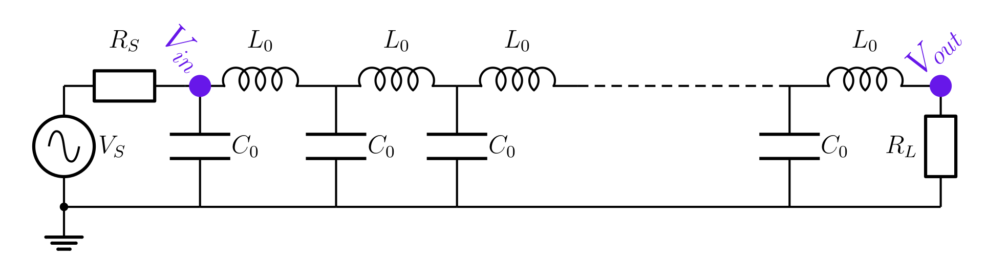
The basic model of a very short length of transmission line is a series inductance per unit length and a shunt capacitance per unit length. A longer length of transmission line consists of many very short sections cascaded together as shown in The line has a characteristic impedance \(Z_0 \,=\, \sqrt{ \frac{L_0}{C_0}\, }\) and a delay per section of \(\tau_s \,=\, \sqrt{L_0 \, C_0\,}\)
The reflection coefficient that is set up when a line of characteristic impedance $Z_0$ is terminated by a load impedance $Z_L$ is the ratio of the reflected voltage to the incident voltage:
\[\Gamma \,=\, \frac{V_{reflected}}{V_{incident}} \,=\, \frac{Z_L\,-\, Z_0}{Z_L\,+\, Z_0}\]Closely related to the reflection coefficient is the return loss, $L$:
\[L \,=\, 10 \log_{10}\left(\frac{1}{| \Gamma |^2}\right)\]The voltage transmission coefficient, $T_V$, is the ratio of the transmitted voltage to the incident voltage while the current transmission coefficient, $T_I$, is in terms of currents. The transmission coefficients are:
\[T_V\, =\, \frac{V_{transmitted}}{V_{incident}} \,=\, 1\,+\,\Gamma ~~~~~~~~~~~~~~ T_I\,=\, \frac{I_{transmitted}}{I_{incident}} \,=\, 1\,-\,\Gamma\]In these experiments an artificial line that is made using series inductors and shunt capacitors is investigated. This models a transmission line quite well provided the delay in each inductor/capacitor section is less than about one tenth of the period of the signal used. The total delay on the line is $\tau_L \,=\, 40\, \sqrt{L_0 \, C_0\,} \,=\, 9.5\,\mu sec$. In free space the propagation velocity is $3\times10^8\,m/sec$ and the $9.5\,\mu sec$ time delay is incurred as a signal propagates over a distance of $3\,\times10^8 \,\times 9.5\,\mu sec = 2.8\,km$. In a typical cable the propagates at about two thirds of the speed in free space so the artificial line models propagation in a cable of length $2\,\times10^8 \,\times 9.5\,\mu sec = 1.9\,km$. This is one reason why an artificial lines is used in a laboratory experiment where laboratory equipment and connection techniques are very limited at high frequencies.
Equipment
Personal computer or laptop with LTspice installed, and perhaps MatLab or Excel.
Preparatory calculations
-
Calculate the characteristic impedance and delay expected along a 40 section line with $L_0 = 47\,\mu H$ and $C_0 = 1.2\,nF$.
-
Calculate the reflection coefficient, transmission coefficients and return loss for load resistances $R_L=2\,k\Omega$, $R_L=385\,\Omega$, $R_L=165\,\Omega$, $R_L=20\,\Omega$, $R_L=2\,m\Omega$ (almost short circuit) and $R_L=200\,M\Omega$ (almost open circuit) on a line with the characteristic impedance evaluated in preparatory calculation 1.
Experiment
In this experiment the artificial line is simulated in LTspice. There are additional damping resistors connected across each of the series inductors to prevent ‘ringing’ in the circuit from masking the main features of the signals. The ringing is caused by the fact that the inductors and capacitors in the circuit form a low pass filter. High frequencies are removed by such a filter leaving a waveform that overshoots and then oscillates, or ‘rings’ towards a final value.
Pulse excitation
-
In LTspice select File and Open to open the LTspice file EE22005_Transmission_Line.asc
The circuit displayed has 40 series inductors and 40 shunt capacitors, excited by a source and loaded by a resistance Rload. The voltage source V1 has an output impedance Rsource whose value is set in the .param statement to $200R$ to model a resistance of $200\,\Omega$. The load Rload is also set here to $200\,\Omega$. This is the matched line case where the source, load and characteristic impedances are equal.
-
Select Simulate and then Run/Pause, or select the green triangle Run, to run the simulation. Then to monitor the input signal hover the cursor over the circuit at Rsource/in node so the red ‘probe’ symbol appears and select this by pressing the left mouse button. The input waveform V(in) shows two pulses with some ‘ringing’ at the leading and falling edges of the pulses. The delay between the pulses is determined by the pulse repetition frequency or equivalently the inter-pulse delay. Also monitor the output pulse by putting a monitor probe at the Rload/out point. The V(out) waveform shows a delayed version of the signals, with more pronounced ringing.
Note the time delay between the input pulse and the output pulse and compare with the expected value of delay through the 40 unit line. Also note the change in amplitude, once the ringing has died away, of the output pulse with respect to the input pulse. Their ratio gives the attenuation of the line, which is typically expressed in decibels.
-
Change Rload to $200e6$ ($200\,M\Omega$) to simulate ‘open circuit’ load condition and run the analysis. Measure the time delay between the two pulses at the input and compare this with the delay between the first pulse at the input and the load pulse. Measure the relative amplitudes of the pulses and determine the reflection and voltage transmission coefficients, and compare to theoretical values.
-
Change Rload to $2m$ ($2\,m\Omega$) to simulate ‘short circuit’ load condition and run the analysis. Measure the time delay between the two pulses at the input and compare this with the delay between the first pulse at the input and the load pulse. Measure the relative amplitudes of the pulses and determine the reflection and voltage transmission coefficients, and compare to theoretical values.
-
Change both Rload and Rsource to $2k$ ($2\,k\Omega$) to simulate mismatch at both the load and the source and run the analysis. Explain the waveforms seen.
-
Set Rload to $2k$ ($2\,k\Omega$) and Rsource to $20R$ ($20\,\Omega$) to simulate another case of mismatch at both the load and the source and run the analysis. Explain the waveforms seen.
CMOS logic circuits powered between $V_{CC}$ and $V_{SS}$ see signals between $V_{SS}$ and $0.3\times V_{CC}$ as logic zero, and between $0.7\times V_{CC}$ and $V_{CC}$ as logic one. When powered between $V_{CC}=3.3V$ and $V_{SS} = 0V$ logic zero is between $0\,V$ and $1\,V$ while logic one is from $2.3\,V$ to $3.3\,V$. Circuit damage can result from inputs at $V_{CC} + 0.5\,V = 3.8\,V$ and at $V_{SS} - 0.5\,V = -0.5\,V$. In the waveforms seen note where signal logic levels could be confused or perhaps cause damage. It may help to scale the voltage source amplitude so that the input pulse amplitude is $3.3\,V$.
If signal or bit rates are increased pulses will be sent more quickly. Reduce the inter-pulse delay from $170\,\mu sec$ and observe the likely effect of increasing the bit rate.
-
It is quite common to consider sources and loads to be ‘matched’ if their return losses are lower than $10\,dB$. Reset the inter-pulse delay to $170\,\mu sec$, set Rload and Rsource to meet this ‘matched’ criteria and observe the waveforms. Can mis-interpretation of logic one or zero states now occur, or cause damage to CMOS circuits? Can the signal or bit rate be increased, and what limits this?
Frequency response
The frequency response of a transmission line could be worked out from the time domain pulse waveforms via Fourier Transforms. The pulse waveforms however do not contain all frequencies. Hence measuring the frequency response directly is often preferred.
-
Right click on the .tran statement next ot the circuit and select AC analysis with Decade sweep, 400 points per decade, start frequency 1e3 ($1\,kHz$) and stop frequency 1e6 ($1\,MHz$). Set both Rload and Rsource to 200R. Run the analysis. On the graph pane delete any unwanted traces and Add trace for $V(in)$, $V(out)$ and the transmission gain, $V(out)/V(in)$. Then remove the phase traces by right clicking on the right hand axis and selecting “Don’t plot phase”. It is now easier to determine the attenuation of the line than in the pulse excitation measurement and see how the attenuation varies with frequency. The influence of the low pass nature of the artificial line is also easy to observe.
-
Change Rload to ‘Open’ circuit and run the analysis. Note the frequency responses and the variation in the transmission gain. Then repeat with Rload set to ‘Short’ circuit.
-
Change Rload and Rsource to $2k$ ($2\,k\Omega$) to simulate the mismatched source and load case, noting the frequency responses and the variation on the transmission gain.
-
Change Rload and Rsource to $385R$ ($385\,\Omega$) to simulate the case where the source and load are ‘just matched’ noting the frequency responses and the variation on the transmission gain. Then change Rload and Rsource to $165R$ ($165\,\Omega$) to simulate the case where the source and load are ‘just matched’ but low, noting the frequency responses and the variation on the transmission gain.
Skills
Characterisation of transmission line electrical performance under matched and mismatched conditions.
Evidence
Source/load conditions and Graphs of $V_{in}(t)$ and $V_{out}(t)$, and corresponding $V_{out}(f)/V_{in}(f)$, under matched, open and short circuit load conditions. 50-100 word explanation of the waveforms.
Source/load conditions and Graphs of $V_{in}(t)$ and $V_{out}(t)$, and corresponding $V_{out}(f)/V_{in}(f)$, under load mis-matched conditions. 50-100 word explanation of the waveforms.
Source/load conditions and Graphs of $V_{in}(t)$ and $V_{out}(t)$, and corresponding $V_{out}(f)/V_{in}(f)$, under source and load mis-matched conditions. 50-100 word explanation of the waveforms.
Observation of data rate limitations. 50-100 word explanation of the data rate limitations.