Skills Mapping
Dr J. G-H-Cater & L. Jabban -
07/03/2024
Skills ? :
Schedule:
Tuesday, Week 25 .
Modular Display Project PCB Layout
The aim of this lab is to produce a PCB layout from the schematic produced last lab. The final PCB must match the requirements outlined below.
Setup
Similar to the previous lab, the first step is ensuring that the libraries are linked correctly.
Setup Exercise: Add the Required libraries
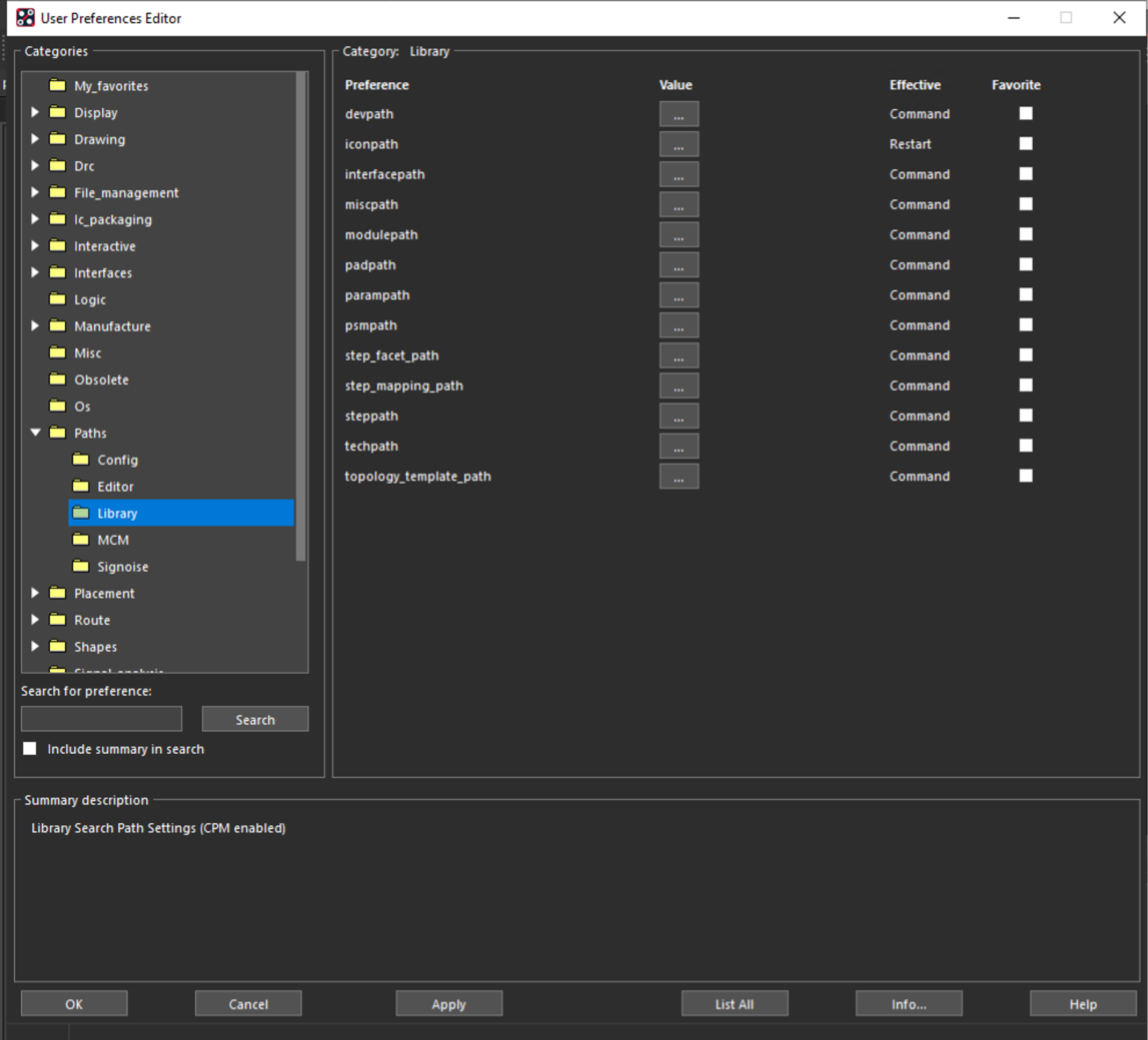
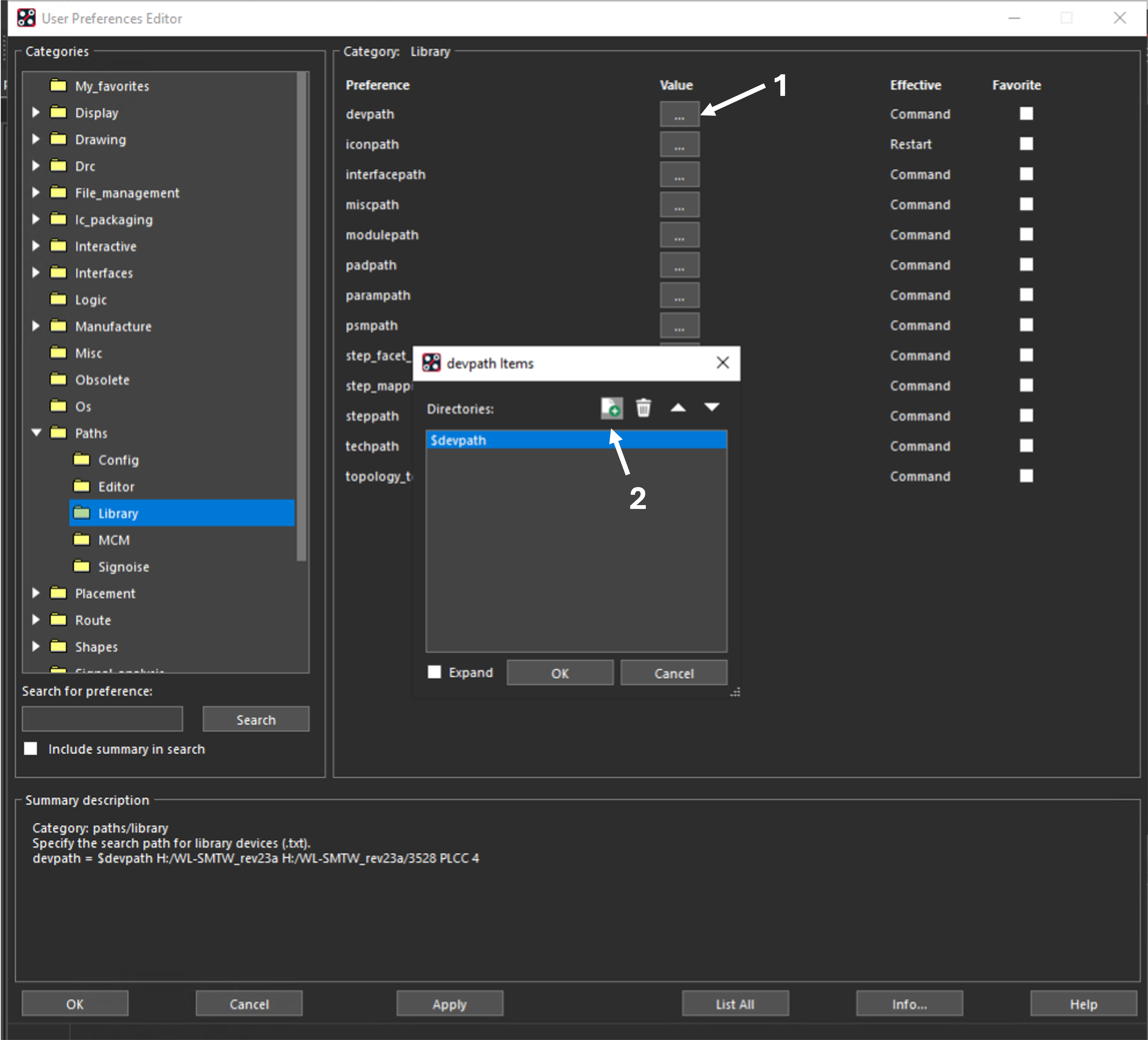
- Navigate to user preferences by clicking on Setup -> User Preferences.
- Select Paths -> Library.
- Add the paths to the libraries to
devpath. You must ensure that you have pointed Allegro to each and every library you are using, listed below in the table. - Repeat step 3 for
padpathandpsmpath.
| Component | Path to correct folder |
|---|---|
| LED | WL-SMTW_rev23a/528 PLCC 4 |
| Arduino | ARDUINO_NANO |
| BSS123 | ul_BSS123-215/AllegroPCBFootprint |
| Tactile switch | WS-TATU_rev19a/THT Tact Switch Right Angle Type with Ground Terminal 6x6 |
You may need to close Allegro and re-open it for the changes to be applied.
Design Requirements
The design requirements are:
- Board Dimensions: The PCB must adhere to specific dimensions provided in the drawing below.
- Component Placement: All surface mount components must be placed on the top of the PCB and all through hole components must be placed on the bottom.
- LED Placement: One LED must be positioned within each designated rectangle on the PCB’s top side, correlating with the locations where acrylic sheets will be placed. This ensures each sheet is appropriately illuminated.
- Arduino Headers Location: Arduino headers are to be positioned on the bottom of the PCB, aligning with a specified area indicated by a rectangle with a dashed outline.
- PCB Layer Restriction: The design is limited to two layers, which is a common choice for simpler circuits that don’t require complex routing or a high number of electrical connections.
- Username: Your username is to be included on the silkscreen layer of the PCB. This enables your PCB to be identified after manufacturing.
- Clearance Areas: Areas highlighted in grey must remain free of any components to enable assembly - this would be a good place to include your username!
- Mounting Holes: While not mandatory, you may include mounting holes to affix the board to an external case.
- Switch Placement: The switch should be incorporated along one of the PCB’s long edges on the front side. This makes the switch accessible for user interaction.
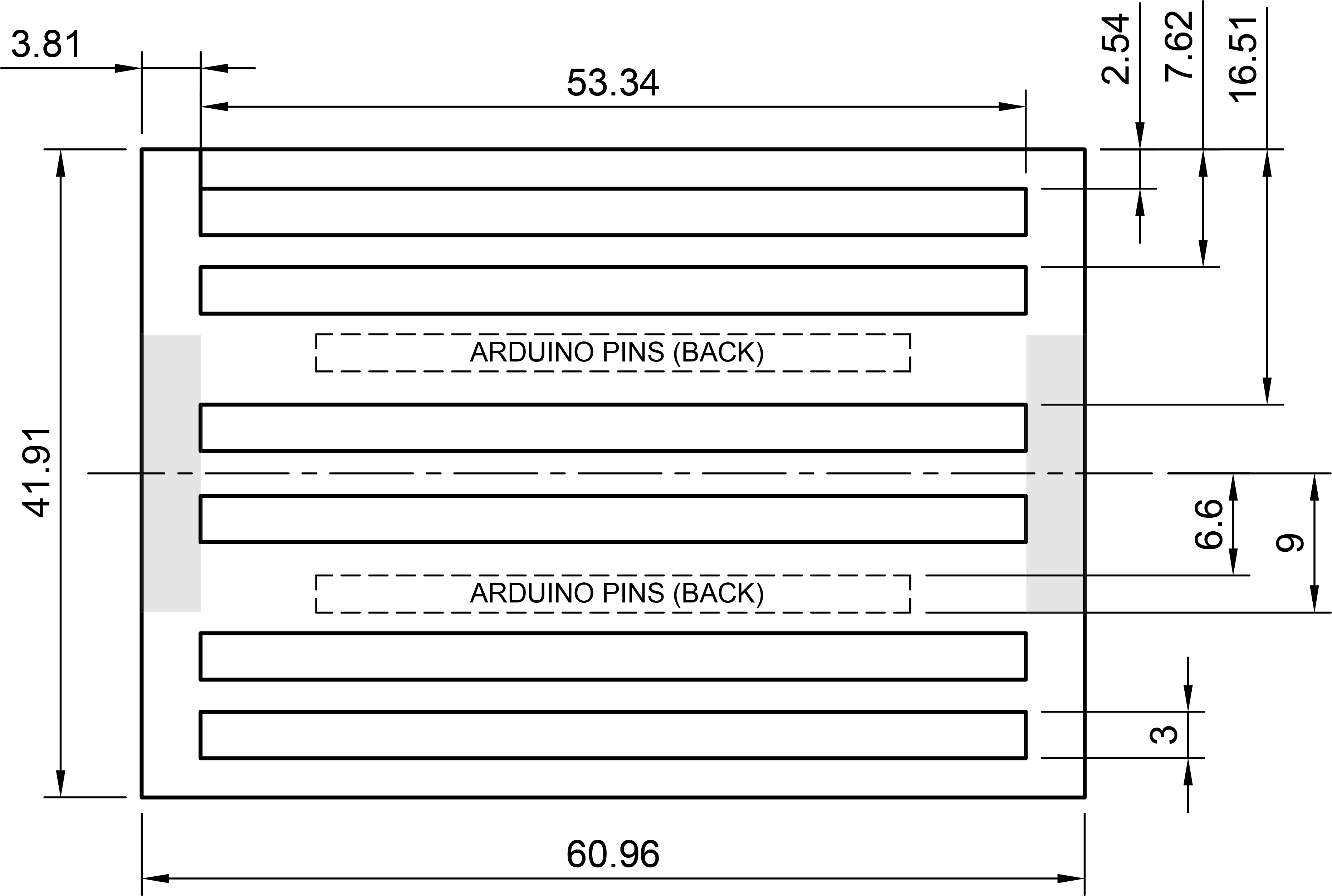
Note that the dimensions are set in multiples of 1.27 for ease of alignment to a 1.27mm grid. Setting the grid to 1.27x1.27mm will make the layout easier.
Useful Information & Tips
- You can use the
Silkscreenlayer (within Board geometry) to add text and shapes that you want printed on the PCB. Note that these must not cross any copper pads. - You can use the
Dimensionlayer (within Board geometry) for drawing shapes to help you with placement and routing. - The arduino footprint is based on the Arduino Nano, not the Arduino Nano ESP32. This should not cause issues in this application, as most pin definitions are identical, but you may wish to compare the datasheets.
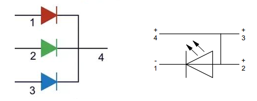
- The LEDs we are using are common cathode LEDs. This means that there are multiple anode pins, but only one cathode pin. On typical RGB LEDs, each anode pin connects to a different colour LED, allowing direct control of each colours brightness. In this case, we are working with single colour LED, so the three anode pins are connected together. This is seen in the datasheet, as shown below on the right of . This is beneficial for us as it means that we can use any of the anode pins when connecting the LED to help make the routing easier.
- The selection of which GPIO pins are used for the LED and switch circuit connections can be chosen according to what is easiest when performing layout to shorten traces and reduce crossover traces. This will require updates on the schematic while you perform the PCB layout to switch the connections to any more appropriate pins. As you do this, make sure not to connect any of the digital IO connections to special pins such as the power or reset pins.
Submitting Fabrication Files
Fabrication files must be submitted on moodle by the 19th of March after being checked.
Further instructions will be added closer to the date.