Surface-Mount Soldering
In this task you will learn to solder surface mount (SM) components.
Surface-Mount Soldering Advice
Reflow soldering is a process in which a solder paste is used to electrically and mechanically bond several electrical components to their contact pads simultaneously. You will learn more about solder paste in year 2 of your degree. Here, you will learn the process of using solder paste to populate a PCB.
The first step is to apply the solder paste on your PCBs pads. Solder paste has a limited shelf-life. The solvent in the solder paste will evaporate over time. At room temperature it will dry after about half an hour and will not be workable after this time. Solder paste should be stored at low temperatures, preferably in a fridge to avoid the solvent evaporating.
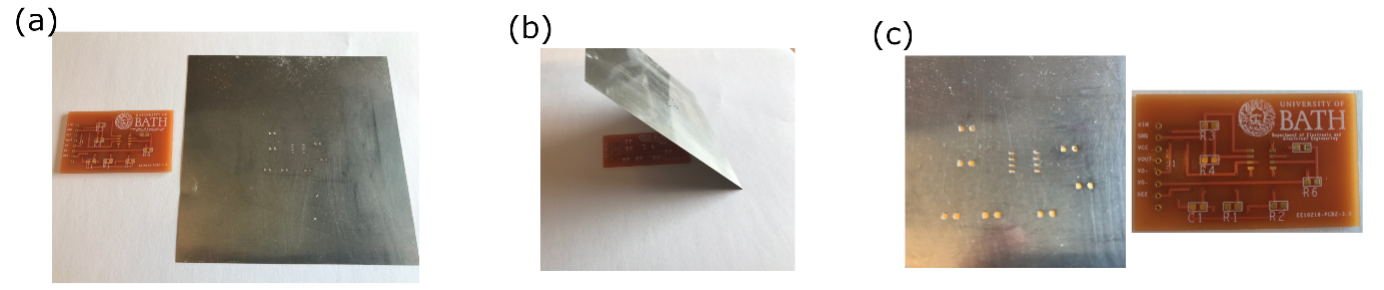
It is a good practice to have all your components to hand before you start populating your PCB. There are several ways you can apply solder paste to your PCB pads. A straightforward, but very time-consuming way is to add solder paste using a syringe or fine paint brush. This approach is very likely to yield poor results. It requires high a very level of dexterity and cognitive focus and is not tractable for PCBs of many hundreds or thousands of pads. A more robust way that is more commonly used in industry is to use a stencil. A stencil is usually made from thin steel, ca. 0.2 mm in thickness, that has been laser cut with the pad pattern, as shown in (a). Mylar or other materials can also be used for this purpose. Stencils provide a physical template for the areas that are to be covered in solder paste. Solder stencils are often bought at the time of PCB production from the same suppliers, though separate stencil suppliers are also available.
To use the solder stencil (often also called “solder mask”), place it on top of your PCB and carefully align it so that the stencil openings align with the PCB pads ((b)). Ensure that the stencil covers the entire PCB except the pads where solder paste is needed (as illustrated in ((c)). Next place a narrow bead of solder paste on one edge of the stencil. Avoid the temptation to add large amounts of solder paste. This is wasteful and will likely result in solder paste ending up on unwanted areas on your PCB. Using a squeegee or bar, draw the solder paste across the stencil, ensuring uniform pressure is applied throughout. After drawing across the entire stencils length, ensure all apertures (holes) in the stencil are covered with solder paste. Now carefully remove the stencil. Using the optical microscopes provided you should be able to see all the pads covered with the solder paste. Once completed, clean the stencil with blue towel and IPA.
We can now mount the components. Solder paste is tacky. SM components have very low mass and the tackiness of the solder paste is sufficient to hold the components in place. Using tweezers or narrow nosed pliers carefully place the components onto the PCB. Very carefully place the populated PCB into the reflow over for heating. Reflow ovens have very fine control over the temperature as a function of time. This is called a thermal profile. The stages of the reflow thermal profile include:
- Pre-heat - to activate the flux
- Soak - to warm the whole board to just below the solder melting point
- Spike - to, as fast as possible, heat the board to above the melting point to reflow the board
- Cool - so that the board can be safely removed without the traces oxidising or harm being caused to the user
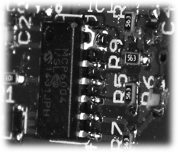
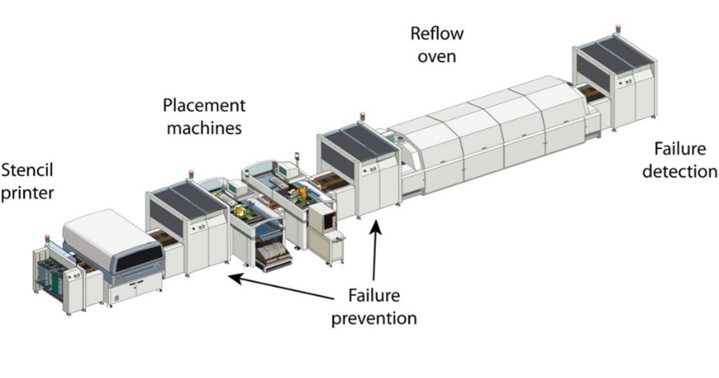
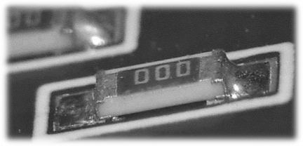
The timings and temperatures are extremely important and are standardised for most solder types. Thermal profiles of specific solder types are often documented in the solders Data Sheet. Different reflow profiles exist for different materials. In today’s lab a standard thermal profile will be used. Once cooled, your SM solder joints should look like . A typical industrial system is shown at the top of this page (), which automates this process.
If you choose to use a syringe or brush, and are a little messy, the soldering reflow is still likely to work! This is because the green coating on the board is designed to ensure the solder flows to the exposed copper pads. The green coating is hydrophobic and surface tension effects during the solder reflow causes the molten solder to move towards the PCB copper pads. It is this affect which causes components to self-align and move in the right direction. Care must be taken however as very small components can often tomb stone during this reflow process. This causes one side of the component to be bonded to the PCB whilst the other points vertically upwards. Tomb stoned components will need to be manually unsoldered and manually resoldered, which can be a very challenging and time-consuming process.
In this laboratory you will learn how to use a reflow oven and the steps required to populate a surface mount PCB.
Lab Exercise
Preparation
In this laboratory, if you do not yet already have one, please collect a small empty component box and label this with your university username using a new white label provided. From the Component Towers please collect, and store in your box, the following:
Instructions
For today’s lab you are required to complete the following activities:
-
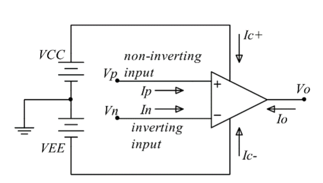
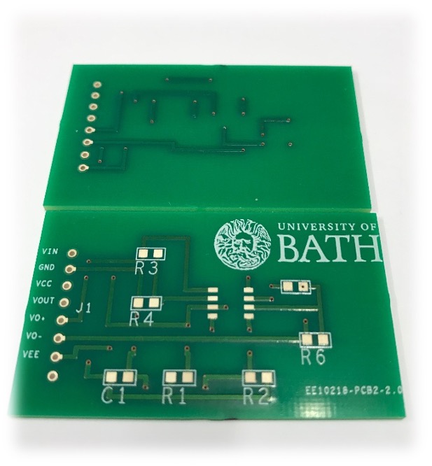
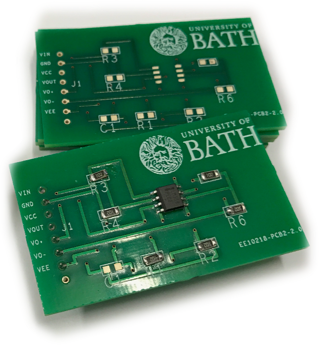
Populate the PCB. To do this solder the SM resistors (SMR) and opamp as described above. The Unit Convenor and GTAs will be located at the reflow ovens to help guide you and answer any questions you may have. Your final board should look like with solder joints like those shown in . Your final board comprises one inverting and one non-inverting amplifier. For more details on the functionality of the circuit please consult your year 1 circuits units.
-
We can now test connectivity of the PCB. This involves checking continuity on the now populated PCB. To test the connections between components we use a digital multimeter (Agilent 34401A 6½ Digit Multimeter). Multimeters are located above the lab desktop PCs. In the boxes provided, find suitable leads, and probe your PCB to ensure all components are soldered securely and have good electrical connectivity. You will be asked to demonstrate this during sign-off.
-
We can now test functionality of the PCB. Open the data sheet for the opamp and using a E3531A Triple Output DC Power Supply (located above the lab desktop PCs) apply power to the board and a DC input voltage and at the input ($V_{in}$). Use the digital multimeter measure the output voltages.
You will be asked to demonstrate this during sign-off.
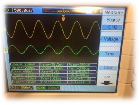
- (Optional: non-credit bearing) - Test your circuit. We can extend our tests by considering AC input voltages (Figure 5). Using a Keysight 33500B Series Waveform Generator (located above the lab desktop PCs) apply a 1 kHz input voltage with an amplitude of 0.5 V to the input terminal. Using leads provided, measure the AC output voltage using the Keysight DSOX1102A Digital Oscilloscope (located above the lab desktop PCs).

Inverting Amplifier equation: $Gain(Av) = \frac{V_{out}}{V_{in}} = - \frac{R_f}{R_{in}}$

Non-Inverting Amplifier equation: $Gain(Av) = \frac{V_{out}}{V_{in}} = 1 + \frac{R_2}{R_1}$