Through-Hole Soldering
In this task you will learn to solder and test through-hole (TH) components. Soldering is an important skill in PCB manufacture. Here, we outline the tools and methodologies necessary for a good soldering technique.
Through-hole Soldering Advice
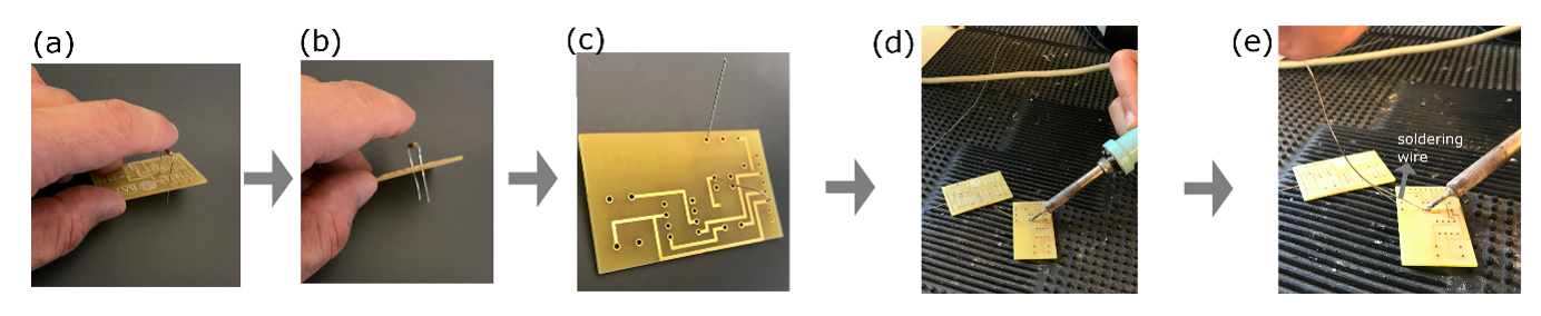
- Push the components leads though their holes as shown in (a), turn the PCB on its back as illustrated in (b) and slightly bend the leads of the components to mechanically hold it in place, as illustrated in (c).
- For soldering irons with a temperature setting / read out, set the soldering iron temperature to around 290°C for lead-based solder or 310°C for lead free solder. You are using lead free solder in this lab. It is possible to use higher temperatures, though in such cases extreme care must be taken to avoid melting the PCB base material or delaminating the copper traces from the PCB.
- Prior to any soldering, ensure you clean the tip on the iron with the damp sponge or brass tip cleaner provided. Do this with the damp sponge sat in the iron holder. Take care throughout this process as the soldering iron is very hot!
- Apply the soldering iron to heat the copper trace on the PCB where you want the solder, as shown in (d).
- Carefully feed a small length of solder (typically less a 2-3 mm) onto the hot junction so that it melts and flows over the pad and the component leads, as illustrated in (e). PCB soldering requires very little solder. It is better to use less solder in the first instance and add more rather than add to much solder and then have to remove this using a solder sucker of solder wick ().
- Once the solder has flowed around the component leads and it has cooled (which takes a few seconds) the joint is made. Joint done! Repeat the process for all remaining joints on the PCB.
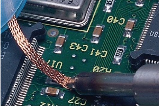
- Should you add too much solder to the joint it may be necessary to remove some. You can do this using the desoldering braid provided, as illustrated in . Heat the back of the braid with the other side of the braid in contact with the solder you would like to remove. The solder will melt and be drawn into the braid. Remove the braid whilst still hot. Take care not to burn yourself. The joint can now be remade using a more suitable amount of solder.
- Solder removal can also be achieved using a solder sucker. Heat the solder until it can be seen to flow, pressurise the solder sucker in your other hand, and carefully bring the tip of the solder suck just above the solder to be removed. Press the suck button and the solder sucker will then remove the solder.
- Once you have completed all of the joints and have repaired any joints that had too much solder on them, next, using sharp snips, trim the component leads on the underside of the PCB.
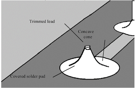
A good soldering joint looks like . The soldering iron has been held against both the component pins and the copper track, ensuring a good joint. The suitable amount of solder has been used with the soldering iron applied for the correct length of time (3 seconds). You are targeting a concave fillet.
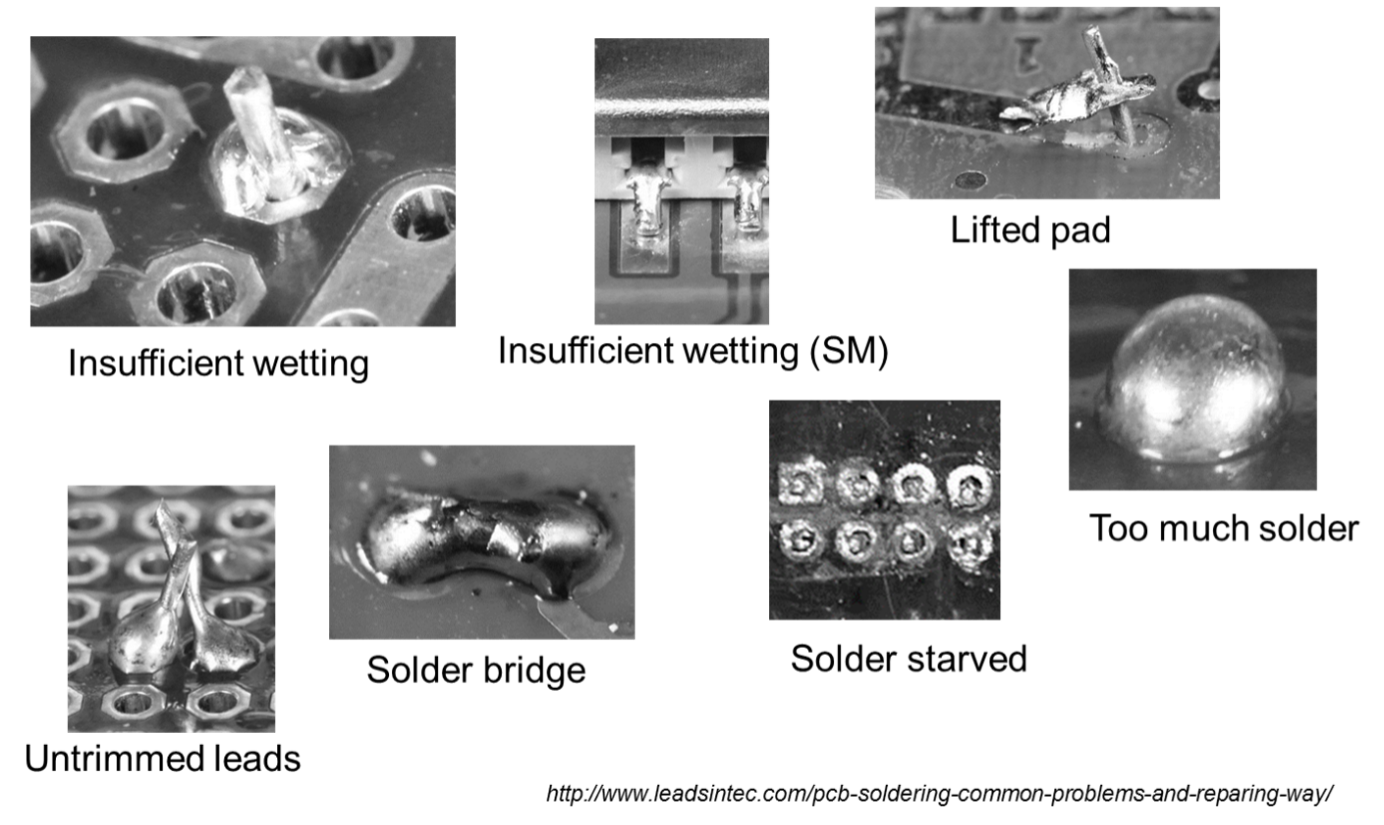
outlines some of the most common soldering issues you may experience and should aim to avoid during when soldering your PCB in the lab.
Lab Exercise
Preparation
In this laboratory, if you do not yet already have one, please collect a small empty component box and label this with your university username using a new white label provided. From the Component Towers please collect, and store in your box, the following:
- 1x unpopulated TH PCB
- 6x TH 1KΩ resistors
- 1x an 8-pin linear header
- 1x 8 way opamp seat
- 1x TH opamp (LM358N)
Instructions
For today’s lab you are required to complete the following activities:
-
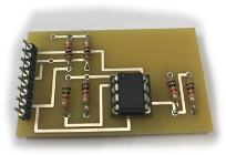
By following the guidance in the Soldering Advice section, above, populate the PCB by soldering the components, as illustrated in .
-
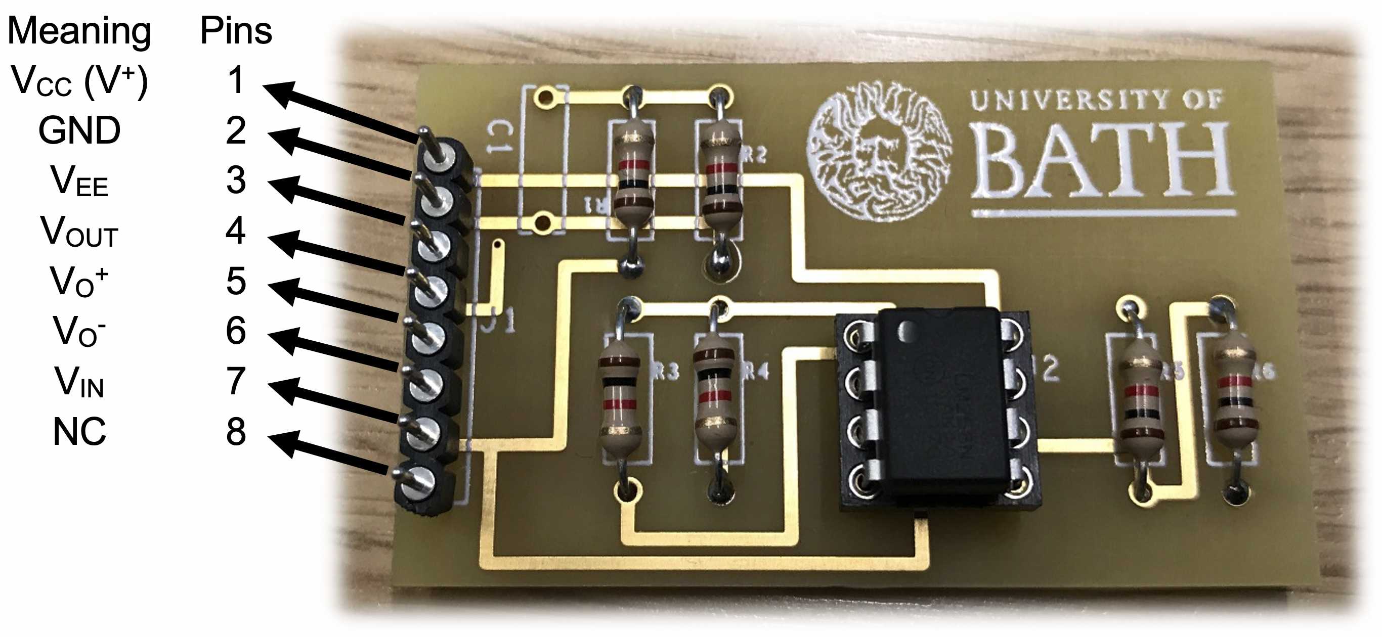
We can now test connectivity of the PCB. This involves checking continuity on the now populated PCB. The pin allocation and schematic of the PCB is given in below to assist in this process. To test the connections between components we use a digital multimeter (Agilent 34401A 6½ Digit Multimeter). Multimeters are located above the lab desktop PCs. In the boxes provided, find suitable leads, and probe your PCB to ensure all components are soldered securely and have good electrical connectivity. You will be asked to demonstrate this during sign-off.
-
We can now test functionality of the PCB. Your board comprises both an inverting () and non-inverting () amplifier. Open the data sheet for the opamp and using a E3531A Triple Output DC Power Supply (located above the lab desktop PCs) apply power to the board and a DC input voltage at the input ($V_{in}$). Use the digital multimeter measure the output voltages.
You will be asked to demonstrate this during sign-off.
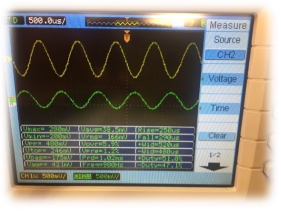
- (Optional: non-credit bearing) We can extend our tests by considering AC input voltages (). Using a Keysight 33500B Series Waveform Generator (located above the lab desktop PCs) apply a 1 kHz input voltage with an amplitude of 0.5 V to the input terminal. Using leads provided, measure the AC output voltage using the Keysight DSOX1102A Digital Oscilloscope (located above the lab desktop PCs).
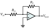
Inverting Amplifier equation: $Gain(Av) = \frac{V_{out}}{V_{in}} = - \frac{R_f}{R_{in}}$

Non-Inverting Amplifier equation: $Gain(Av) = \frac{V_{out}}{V_{in}} = 1 + \frac{R_2}{R_1}$