Getting started with SystemVerilog
Creating a SystemVerilog project in Altera using Quartus Prime and Questa
This is a quick guide to setting up the software environment required to use the Altera DE1-SoC boards for EE12001 Design skills. These boards contain a Field Programmable Gate Array (FPGA) which is basically lots of logic gates with reconfigurable wiring between them. The process of designing circuits for use on an FPGA is very similar to the process designing custom silicon chips, but because an FPGA can be re-programmed, the design process is fast and cheap in comparison to the huge sums of money spent on custom devices. It is now very unusual for discrete logic (e.g. 74 series devices) to be used in newly designed products as the lowest cost programmable devices are just as cheap and small.
This guide is deliberately very brief. There is far more that can be learned about the tools. However, what we are interested in is learning how to design digital systems and how to write SystemVerilog because it is a vendor independent language for describing digital systems.
The Altera DE1-SoC board
You will be using the Altera DE1-SoC educational board as shown in . Note the location of the switches, push buttons and LEDs. These will be the first I/O devices you use.

Getting started
Use sections 1 to 4 to get your environment set up. You can then type in the code described in the appropriate tutorial document. Once you have the SystemVerilog code typed in, follow sections 5 and 6 to implement your design into the FPGA.
1. Open Quartus Prime.
Open the design tools by selecting:
Start » Intel FPGA 22.1 » Quartus (Quartus Prime 22.1)
This is the development tool provided by Altera. It is possible to use other tools from independent software vendors, but the Altera tools are fine for our purposes.
2. Set the project name and location
Click New Project Wizard and then click Next in the pop-up until you reach the dialog box for entering the project location and name. See .

Create a directory to work in (e.g., h:\DSDprojects), then create a folder for the corresponding tutorial (e.g., h:\DSDprojects\tutorial1), set the project name (e.g., tutorial1) and the name of the top level module or entity (e.g. tutorial1) as shown in . Make a note of this module name as it is important that it matches the code written later.

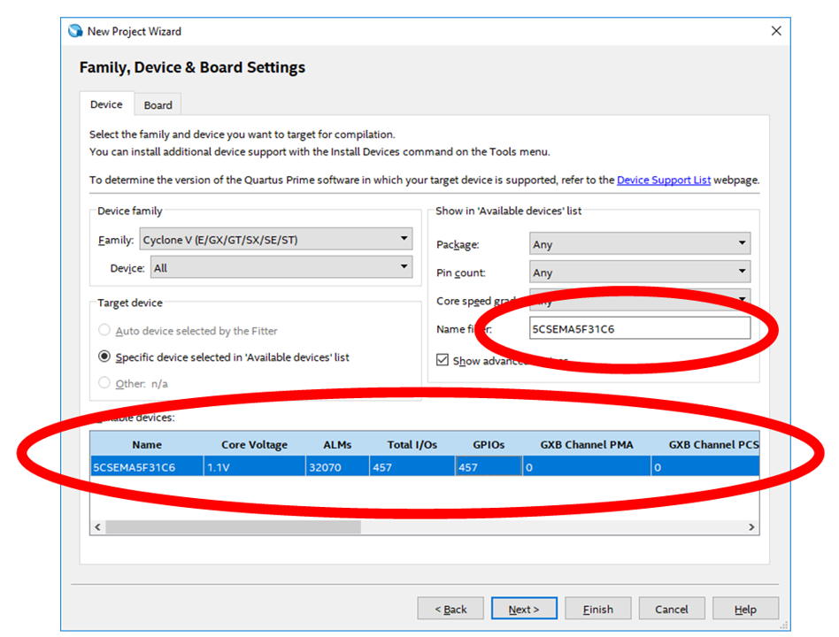
3. Set the device type
Click Next until you get to the Family & Device Settings dialog. The FPGA we will be using is a 5CSEMA5F31C6. Type this value into the search box. Select the correct device from the list of available devices as shown in . Click finish to end the set up wizard. You have now created an empty project that you can use to create SystemVerilog designs.
4. Create a SystemVerilog module
Select File » New from the menu and then select SystemVerilog HDL File from the dialog box that appears ().
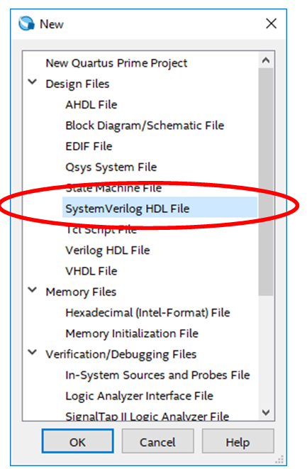
In the tutorials this is the procedure you will use to type your SystemVerilog code into. You can use this method to create multiple design files and testbenches.
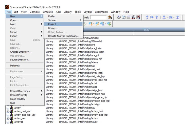
5. Simulate a module using Questa Intel FPGA
Start the simulator by selecting:
Start » Intel FPGA 22.1 » Questa Intel FPGA
Start by creating a new project by selecting File » New… » Project… as shown in .
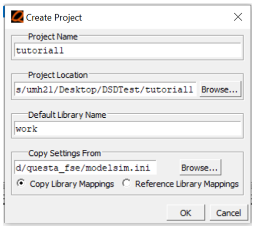
Then, you will see the Create project window. You need to enter the project name, e.g., tutorial 1, and select the folder of your project, where you have the files that you need to simulate. The Default library name should be left as work and then do click on OK, as shown in .
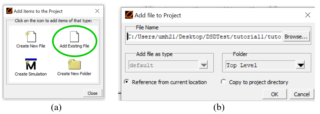
You will see the window named Add items to the project, where you need to select the Add Existing File option as shown in a. When you click on Add Existing File you will see the window shown in a, where you need to select the files that you will simulate (e.g., tutorial1.sv and tutorial1_tb.sv) and click on OK.
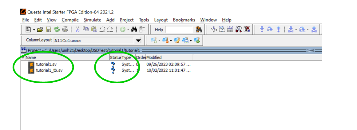
After this step, you should see the files for simulation added in the project as shown in . The question mark symbol in the status column indicates that these files are not compiled yet.
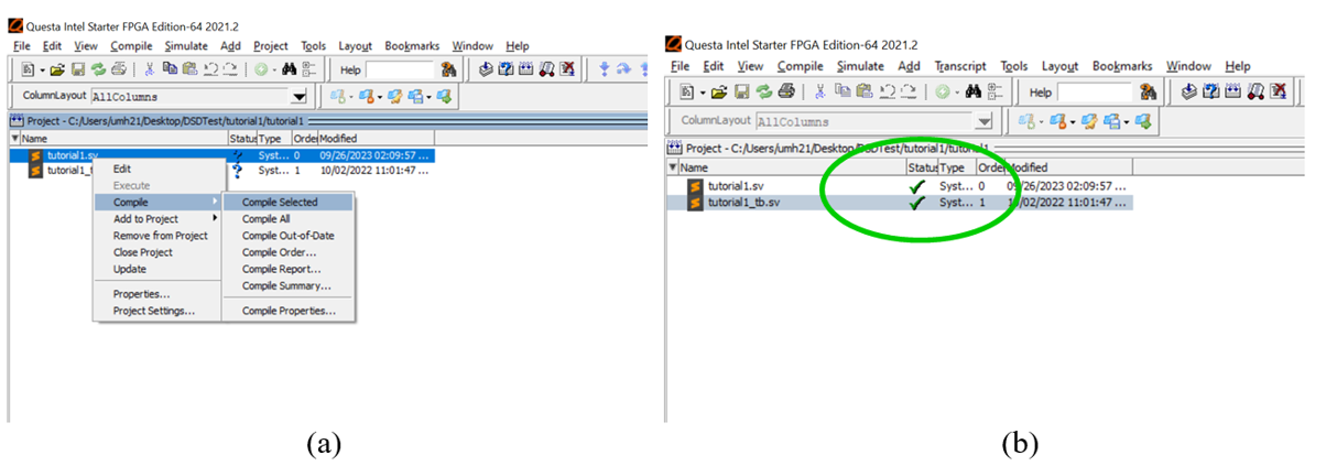
Right click on each file and select the option Compile » Compile Selected… as shown in a. If the compilation process is correct, then you will see a green tick in the status column as shown in b.
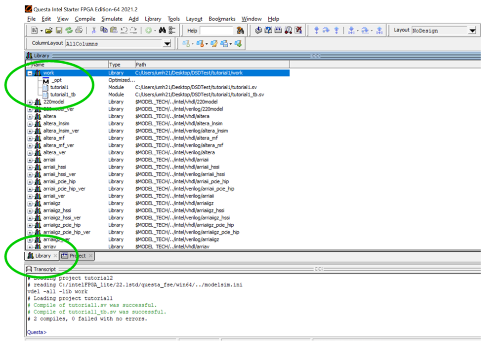
The next step is to click on the Library tab at the bottom of the window as shown in . You will see that the work folder has been created and contains the files compiled in the previous steps.
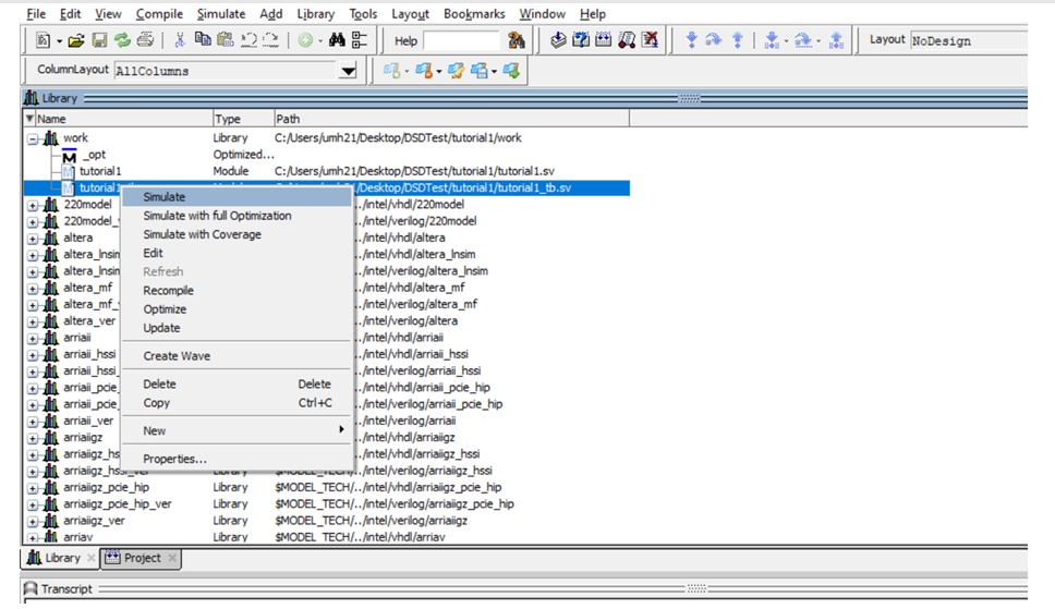
Now, right click on the testbench file (e.g., tutorial1_tb), which is the file that is used to simulate the functionality of the actual digital system (e.g., tutorial1). Then, select the option Simulate as shown in .
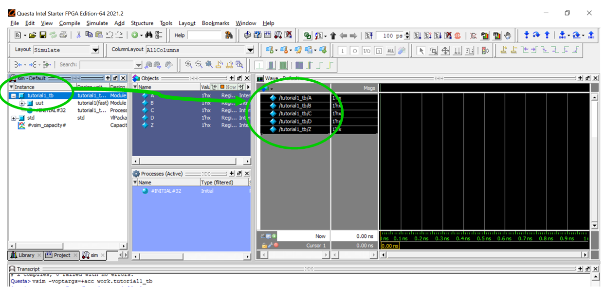
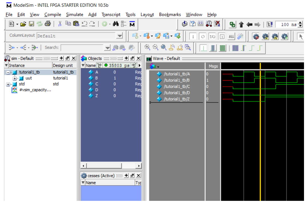
Then, you will see the window shown in which contains the module, signals and wave sections that will be used to run the simulation and observe the output signals of the design digital system. You need to click and drag and drop the testbench located in the Instance panel to the Wave panel as shown in .
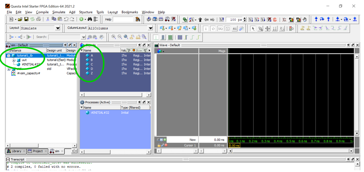
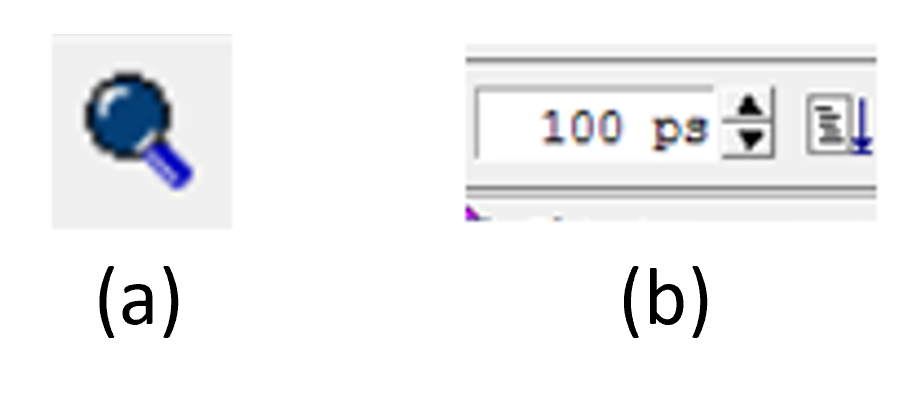
There is a large number of buttons at the top many of which are only enabled when the Wave window is selected. The most useful ones are shown in .
The cursor in the Wave window can be used to examine the signal values at a given point in the waveform.
Once your design simulates correctly you can synthesise it for the FPGA.
6. Create an FPGA programming file
In order to use a SystemVerilog design, we must tell the tools which pins on the FPGA are connected to the physical objects on the board like the switches and LEDs.
- In Quartus, select Assignments » Import Assignments.
- Click on the button marked (…) and select the appropriate file for the tutorial (e.g. SimpleCombinatorial.qsf for tutorial 1). See the links to the zip files in the following pages.
- Select OK on the Import Assignments dialog box. The effect of this import is to map module inputs and outputs to the correct FPGA pins. For example, SimpleCombinatorial maps signals called A, B, C, and D to the push buttons marked KEY3 to KEY0 respectively on the FPGA board. It also maps signals Z to LEDR0 respectively on the board.
All the information has now been input to the tools. In the lower left part of the Quartus window there is a window marked as Tasks. In this window do the following:
- Make sure that Compilation is selected in the Tasks window.
- Double click on Compile Design. Once this is complete, the main sections will have a green colour tick by them.
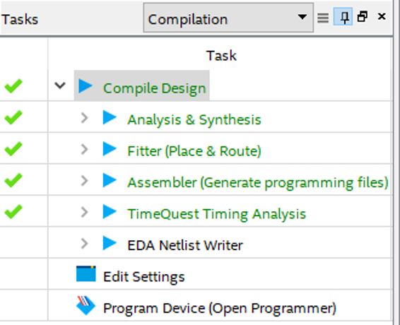
If you made any errors in typing in the code above, the tools will complain. You can double click on the errors to go to the relevant line. Syntax errors are often in the line immediately preceding the line that produces the errors. Go back, fix the design, save it and compile again. This compilation process creates a .sof file in the output folder of the project directory that you can use to program the FPGA board.
7. Programme the FPGA
Once the tools report that the assembly was successful you can move on to programming the FPGA board. First set up the board itself doing the following:
- Connect the FPGA board to its power supply.
- Use a USB cable to connect the FPGA to the front USB port of the PC.
- Press the red button near the power supply connector and the blue power lights should come on. A test programme may start up depending on how the board was configured.
The board is now configured and ready for use. You now need to load your design onto the FPGA as follows:
In the Task window of the Quartus software, double click on Program Device (Open Programmer). This will open the programmer window and you can now download the design to the DE1-SoC board.
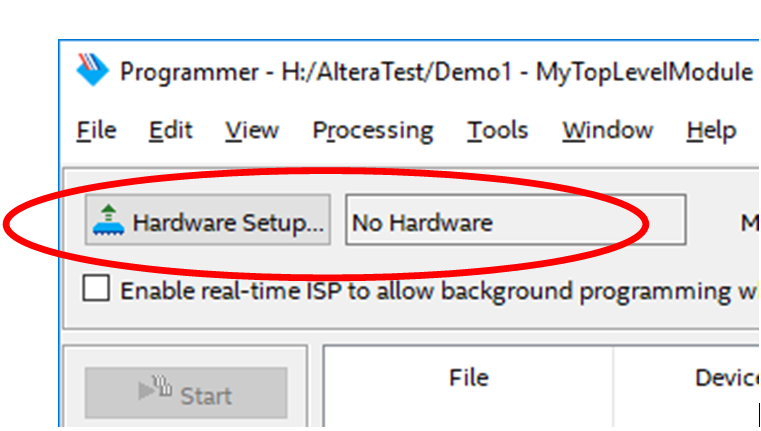
Double click on the USB-Blaster entry from the list of available hardware items and then click close. The No Hardware notification should now change to DE-SoC.
Click on the Auto Detect button in the programmer window. Select the 5CSEMA5 as the device type and click OK.
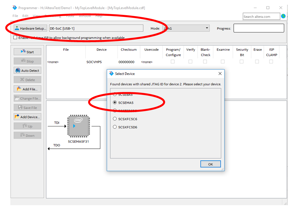
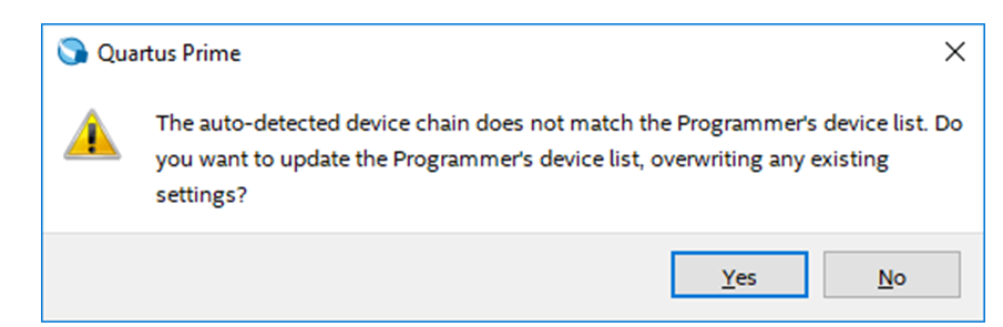
Click Yes if the following warning appears.
Double click on the word <none> on the second line and select your .sof file generated from part 6. Select the Program/Configure box and press the Start button to program the FPGA.
You can now test your design. If you are using the push buttons, remember that they produce logic 1 when NOT pressed.