Characterisation of an Up-converter
Introduction
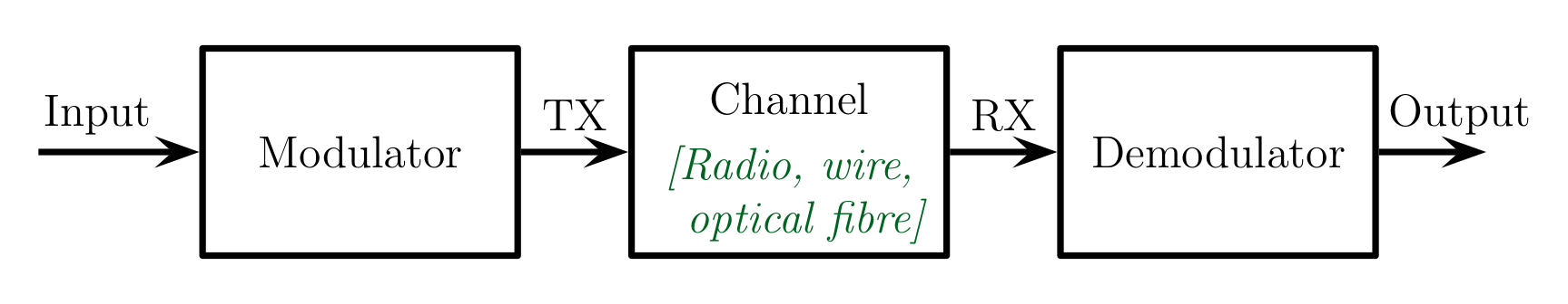
The aim of this experiment is to help students gain familiarity with an upconverter. In a common configuration for communications links and measurement equipment an upconverter takes in base band frequency data and modulates this onto a high frequency carrier forming the transmission signal TX. This is sent over a channel in radio waves, as signals on wire cables or as an optical signal on a fibre. At the receiver the high frequency received signal RX is down converted back down to base band frequencies.
This experiment focuses on the characterisation of the upconverter modulator and the features the circuit produces. The experiment, which should be recorded in real time, assumes a basic theoretical knowledge to the level taught in the EE22004 and EE22005 courses. The lecture notes for these courses are available on Moodle.
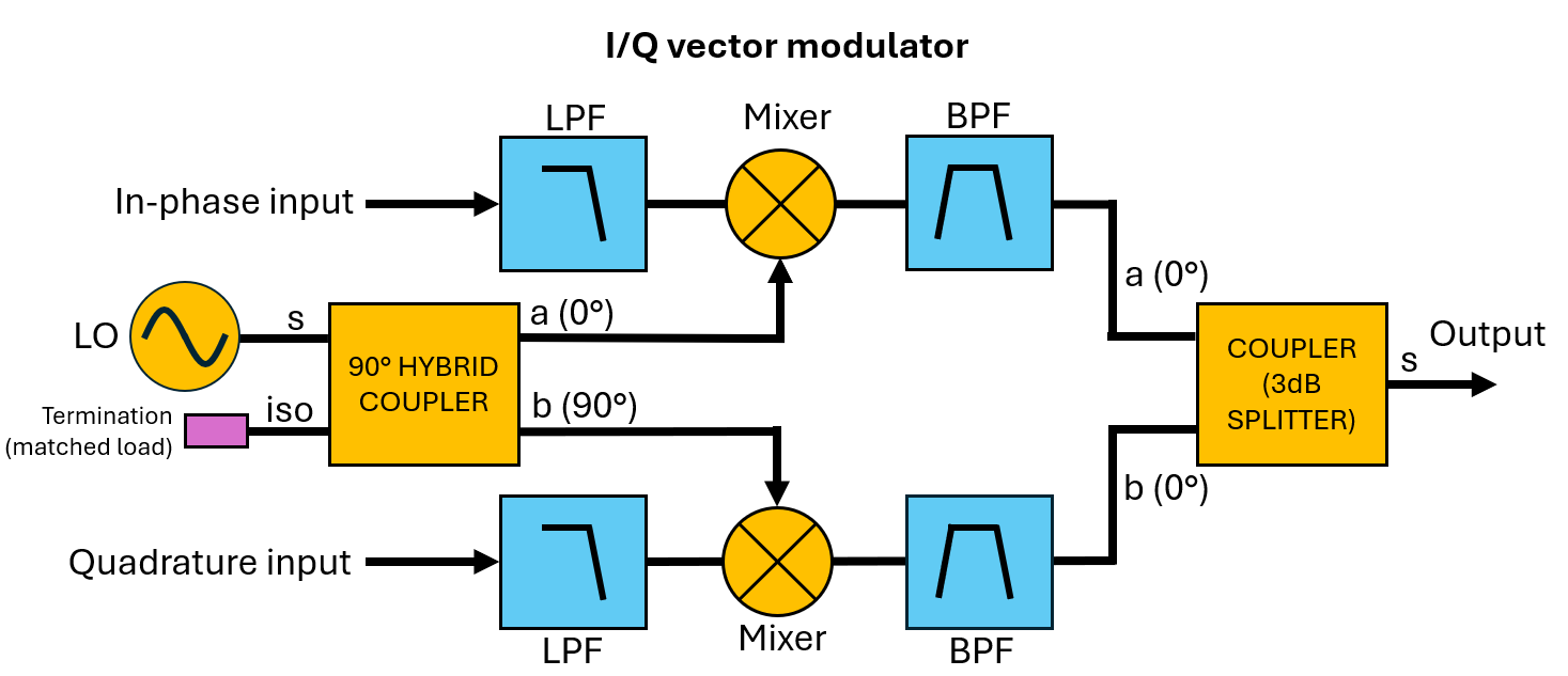
The upconverter has two channels, the I and Q channels. These are formed by driving mixers in-phase and in phase quadrature with a local oscillator (LO) signal. The two LO signals are formed by driving a hybrid quadrature coupler with the LO signal. The outputs of the mixers are filtered to remover unwanted intermodulation products, just leaving the desired sum or difference frequency signals. The I and Q channel signals are combined in equal proportions by the output, equal phase and amplitude, combiner.
List of Experiments and Recording
In this experiment you will be examining the upconverter by first examining the sub-circuits that comprise the upconverter and then the complete upconverter. You will be looking at:
-
Hybrid power splitter.
-
Hybrid coupler.
-
Balanced Mixer.
-
Band pass filter.
-
Upconverter.
There should be sufficient time in the three hour laboratory sessions for all measurements to be taken, recorded graphically where needed, and discussion of the results developed. You need to keep a log of your experiment capturing all of your results, analysis and discussion, with sufficient detail to allow repetition of your experiment.
Please note that while it is basic laboratory technique to record as much data as possible in real time, many students choose to complete their graphs and complement their discussion and conclusions in their log after the event, and this is perfectly acceptable. A formal written report is not required, but your log is the basis of the information needed to provide evidence of attaining various levels of skills in Mahara.
Preparation before beginning the experiments
-
Read through this Laboratory Script to familiarise yourself with what is to be done during the experiment.
-
Go through the quick introduction to LTSpice in the video file EE22005: A quick introduction to LTSpice for Comms Lab activities on the EE22005 Moodle page under “Communications Engineering Laboratories”.
Tests
The sub-circuits and complete Upconverter are already set up in files for LTSpice to use. LTSpice is installed on the PCs in the Keysight Laboratories. These LTSpice files are in EE22005_Upconverter.zip on the EE22005 Moodle site under “Communications Engineering Laboratories”, which you should download and unpack into a suitable folder on your H-drive.
Initialise LTSpice by selecting LTSpice in the Windows Start menu. You do not need to share Usage Data in this experiment so select No when asked about sharing.
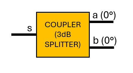
Hybrid splitter/combiner
The hybrid splitter/combiner has a signal s at one port and two equal signals a and b at the other two ports. In a splitter s is split between a and b while in a combiner s is the result of combining a and b. In an ideal case the power splits equally in two parts, so the outputs are 3dB below the input level.
Hybrid splitter/combiner transient response
- Select File and Open to open the LTSpice file EE22005_3dB_coupler_transient.asc
The circuit displayed should show a voltage source, the inductors, capacitors and resistors of the hybrid splitter, and two $50\,\Omega$ resistors connected to ground at the two outputs of the circuit.
- Run the simulation by selecting Simulate and Run/Pause or by selecting the green triangular Run icon. There should then be an additional, but blank, window called EE22005_3dB_coupler_transient.raw. This is where the graphs of data traces will appear.
- To create the data trace for the source input, shown as s on the schematic, hover the mouse cursor over (or near) the connection ‘wires’ near s on the schematic. The cursor will turn into a ‘probe’ icon and left clicking will create the trace in the .raw window.
- Add probes at the outputs a and b on the schematic. As the circuit is balanced the outputs a and b are equal, so only the last trace is visible in the ‘.raw’ window. Data values can be read from the traces by hovering the mouse icon over the trace and reading x and y values at the bottom left corner of the LTSpice window. Using this can be rather time consuming.
-
Press Control-L on the keyboard and the log file opens. This contains the harmonic components of the signals a and b in amplitude and phase. Note that the Normalised amplitude and phase are not very useful in this experiment.
At the bottom of the log file the RMS values of the signals at s, a and b.- Calculate the relative size of a with respect to s in decibels and the note the phase of the fundamental component of a. Note the departure from the ideal value.
- Calculate the relative size of b with respect to s in decibels and the note the phase of the fundamental component of b. Note the departure from the ideal value.
Then close the log file window
- Modify the inductance L1 by right clicking on inductor L1 in the schematic and changing the value of Inductance to $1.5\,\mu H$ and then re-simulate. The V(a) and V(b) traces now differ in amplitude and phase. Confirm the differences in the data in the log file using Ctrl-L.
- Close the schematic (.asc) and output (.raw) windows.
Hybrid splitter/combiner frequency response
- Open the LTSpice file EE22005_3dB_coupler_ac.asc. This is set up to run an AC analysis rather than the transient analysis used in the last section.
-
Run and add probes at s, a and b. In the .raw window there should be solid traces for amplitudes and dotted traces for phases as a function of frequency from 2MHz to 18MHz. As the circuit is symmetric the data for a and b will be identical.
The circuit was designed to operate at 10 MHz. Needing to use preferred values for the inductors and capacitors results in a slight shift in the frequency where the outputs a and b are 3dB below the input s. Note any departure from the ideal values.
-
Change L1 to 1.5uH (click on the inductor, change the value) and Run again. The traces for a and b are now visibly different.
- Close the schematic (.asc) and output (.raw) windows.
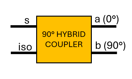
Hybrid quadrature coupler
The hybrid quadrature coupler should split the input signal into two outputs that are equal in amplitude but in phase quadrature. To do this the hybrid quadrature coupler can not just consist of lossless inductors and capacitors, but has to have some resistance in the circuit. It also has an Isolated output where there should be no signal present.
-
Open the LTSpice file EE22005_3dB_hybridcoupler_transient.asc.
-
Run the analysis and set probes at s, a, b and Iso.
The traces a and b show the quadrature nature of these signals. In a perfect design the output signals a and b are in phase quadrature and there is no signal seen at the Iso (Isolated) output. This circuit was again designed for use at 10 MHz, and in using preferred values it is not quite perfect.
-
Examine the .log file (use Ctrl-L) and note the phase difference between Phase (not relative phase) of V(a) and V(b). Note any departure from ideal values.
-
Calculate the ratios in decibels of signal V(a) with respect to V(s), of V(b) with respect to V(s), V(Iso) with respect to V(s) from the RMS data at end of the log file.
-
Change L1 to 1.5uH and re-run. Note the change in the relative amplitudes of V(a), V(b) and V(Iso) in decibels and the phases of V(a), V(b), and V(Iso).
- Right click on .tran in the schematic. Change:
- To AC Analysis
- Type of Sweep is Linear
- No of points is 1000
- Start to 2e6
-
Stop to 18e6
Run the analysis and using the mouse pointer cursor and the values indicated at the bottom left of the window note the amplitude balance and phase balance in the output signals at 6 MHz, 10 MHz and 14 MHz. Note any departure from ideal values.
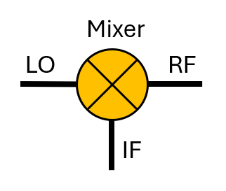
Mixer
The mixer circuit multiplies the input signal at frequency $f_1$ and the local oscillator (LO) signal at frequency $f_{LO}$ to produce an output whose frequency is at $f_{LO} \pm f_1$.
-
Open EE22005_bare_mixer_transient.asc. This models a double balanced mixer that uses a centre tapped transformer.
-
Run the simulation and add probes to monitor the rf, lo and if signals.
The traces are very compressed. To zoom in on part of the wavefrom put the mouse cursor on the data graph, left click and hold and then drag the mouse cursor to include the area of the graph that is desired. Zoom in on the data to cover about $8\,\mu sec$ to $9\,\mu sec$. The 14MHz the V(LO) trace is very smooth. The V(RF) trace is the smallest and almost discontinuous where the diodes switch on and off. The V(IF) trace is approximately sinusoidal at 10MHz but with intermodulation products at other frequencies.
-
Open the log file by typing Crtl-L and record the RMS voltage of the V(RF), V(LO) and V(IF). From that determine the conversion loss in decibels between the IF to RF ports.
-
Investigate the frequency content of the signals:
- Right click on the data trace window and select Zoom to Fit
- Right click on the data trace window and select View, FFT, OK, and in Select Visible Waveforms select all 3 waveforms. This gives the whole frequency spectrum of the signals.
- Right Click on Frequency axis legend and then
- Untick Logarithmic
- Set Left to 0
- Set Tick to 2M
-
Set Right to 80M.
The LO signal is at 14MHz, the IF signal is at 4MHz and the resulting RF signal produced is at 10MHz and 18MHz. Observe that other intermods are present. Measure the amplitudes of the LO, IF and RF(LSB) and RF(USB).
- At the top of the .raw window Right click on IF and LO traces to delete them so that just the RF signal remains.
-
Observe the outputs at the frequencies $\pm n\, f_{RF} \pm m\, f_{IF}$ where $n$ and $m$ are integers.
-
Using the cursor to read off values from the graph determine the dBc of the system - the decibels between the desired RF output and the next highest tone in the frequency spectrum.
-
Record the frequency spectrum by right clicking in the graph and selecting Copy Image to Clipboard. Then open Paint and Paste to copy the image from the Clipboard into Paint. Then Save as a graphic file (.png?) in your H-drive.
-
Conversion loss and drive level
- The conversion loss is the ratio $V_{RF}/V_{IF}$, and this can be affected by the LO drive level $V_{LO}$. Running the analysis and examining the log file (using Ctrl-L) note the amplitudes $V_{RF}(LSB)$ and $V_{RF}(USB)$ and the output $V_{IF}$. Further, evaluate the conversion loss in decibels.
- Change the LO voltage to (0.7, 0.6, 0.5, 0.4, 0.3, 0.2, 0.1)V and measure the conversion loss in decibels for each LO drive level.
- Plot the conversion loss in decibels as a function of the LO drive level in dBW or dBm.
- Close the windows in LTSpice in preparation for the next part of the testing.
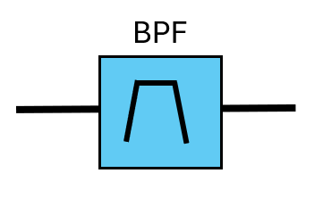
Band pass Filter
The band pass filter prevents the transmission of low and high frequencies while allowing transmission of mid frequencies.
- Load LTSpice file EE22005_RF_BPF_ac.asc
- Run the simulation and set the monitor points to be in and out.
- Right click in the .raw window and select Add Traces. At the bottom of the window in Expressions(s) to Add and type in V(out)/V(in).
- Determine the 3dB bandwidth of the filter and the loss of the filter at 4MHz and at 14MHz.
I/Q up-converter
The I/Q up-converter has an I channel whose mixer is driven in-phase with the local oscillator (LO) and a Q channel whose mixer is driven in phase quadrature with the LO. Band pass filters remove harmonics and intermodulation products so just the desired signal is passed to the combiner at the output, where the I and Q channel contributions are combined equally.
- Load the file EE22005_vectormod.asc into LTSpice.
- Run the simulation and set the monitor points to be in and rf.
- To investigate frequency content:
- right click in the .raw plot window, select Zoom to Fit
- Right click in the .raw plot window, select View and then FFT. Make sure V(in) and V(rf) are highlighted and then click OK.
- In the Select Visible Waveforms window that opens select both waveforms. This gives the whole frequency spectrum for both waveforms.
- Right Click on Frequency axis legend. Then:
- Untick Logarithmic
- Set Left to 0, tick to 2M and Right to 80M.
You should now be able to see the LO component at 14MHz, the IF at 4MHz and the RF LSB at 10MHz and USB at 18MHz. There should be some other intermodulation products as well at frequencies $\pm n\, f_{RF} \pm m\, f_{IF}$ where $n$ and $m$ are integers.
- Measure the amplitude and phase of the IF, RF(LSB) and RF(USB) signals from the log file (Ctrl-L).
- Record the frequency spectrum plot by right clicking in the graph and selecting Copy Image to Clipboard. Then open Paint and Paste to copy the image from the Clipboard into Paint. Then Save as a graphic file (.png?) in your H-drive.
Transfer function evaluation.
The transfer function relates the output at the rf port to the in phase base band input i and quadrature base band input q. For each combination of V(i) and V(q) the output V(rf) is measured. The logical inputs 0 and 1 map to voltages 0.0V and 0.3V at inphase, V2, and quadrature, V3, inputs.
- Set the input state (1,0) by right clicking on the inphase source and setting the Amplitude to 0.3 and right clicking on the quadrature source and setting the Amplitude to 0.0
-
Run the analysis, and from the log file (Ctrl-L) note the amplitude and phase of the V(rf) output. Determine the value of the transfer function
\[H = \frac{RF}{I\,+\,j\,Q} = \frac{|RF| ~\angle(RF)}{|I+jQ| ~\angle(I+jQ)}\] - Repeat the measures and evaluations of \(H\) for the (I,Q) inputs (1,1), (0,1), (-1,1), (-1,0), (-1,-1), (0,-1) and (1,-1). Note how the magnitude and phase of the input relates to the magnitude and phase of the RF output of the modualtor.
| I | Q | V(I) | V(Q) | |I+jQ| | Arg(I+jQ) | |V(RF)| | Arg(V(RF)) | |H| | Arg(H) |
|---|---|---|---|---|---|---|---|---|---|
| (Volts) | (Volts) | (Volts) | (Degrees) | (Volts) | (Degrees) | (Degrees) | |||
| 1 | 0 | 0.3 | 0.0 | 1.0 | 0.0 | ||||
| 1 | 1 | ||||||||
| 0 | 1 | ||||||||
| -1 | 1 | ||||||||
| -1 | 0 | ||||||||
| -1 | -1 | ||||||||
| 0 | -1 | ||||||||
| 1 | -1 |