Characteristics of Operational Amplifiers in Simple Linear Feedback Circuits
Introduction
The aim of this experiment is to help students gain familiarity with the use and application of operational amplifiers in simple linear feedback circuits of practical importance. This experiment focuses on the characterisation of linear features of the amplifier, where the output is not distorted. The experiment, which should be recorded in real time, assumes a basic theoretical knowledge to the level taught in the EE22004 course. The lecture notes for this course are available on Moodle.
List of Experiments and Assessment
In this experiment you will be examining :
-
Inverting amplifier;
-
Non-inverting amplifier;
-
Low Pass filter inverting amplifier.
There should be sufficient time in the three hour laboratory sessions for all measurements to be taken, recorded graphically where needed, and discussion of the results developed. You need to keep a log of your experiment capturing all of your results, analysis and discussion, with sufficient detail to allow repetition of your experiment.
Please note that while it is basic laboratory technique to record as much data as possible in real time, many students choose to complete their graphs and complement their discussion and conclusions in their log after the event, and this is perfectly acceptable. A formal written report is not required, but your log is the basis of the information needed to provide evidence of attaining various levels of skills in Mahara.
Preparation before beginning the experiments
You should have access to and be familiar with the following standard laboratory instruments:
-
DC power supply
-
Signal generator
-
Digital oscilloscope
-
Digital multimeter (DVM)
-
Box/tray of short wires for interconnecting items
-
Box/tray of components including operational amplifiers, resistors and capacitors.
In addition you will be provided with a prototyping board and you should be familiar with its use and built in connections. Typical supply voltages for the op-amp you will be using (LM-741, TL-081 or equivalent) are ±15 V.
The signal generator provides sinusoidal, rectangular and triangular waveforms at a frequency that is variable (programmable) over several decades. The lower limit of the amplitude range of the generator is 20 mV and its output resistance is $50\,\Omega$ (note this can’t be changed). When the signal generator is connected to a $50\,\Omega$ load the voltage applied to the load is half of the source voltage. When connected to an open circuit or very high impedance load the load voltage is the source voltage.
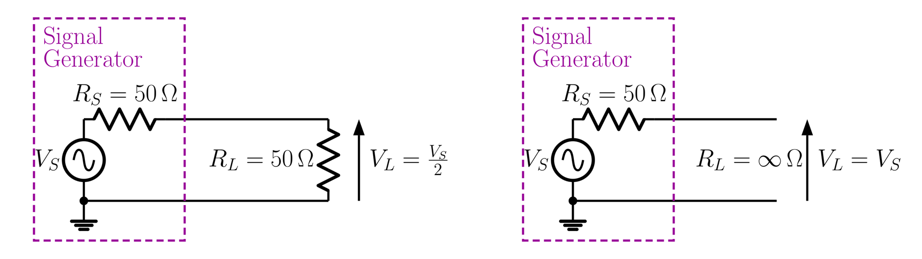
There is a menu setting on the signal generator where you set what type of load impedance is connected to the generator. When set to ‘Low Z’ the signal generator assumes that a low impedance, $50\,\Omega$, is connected and the readout of the voltage is appropriately scaled to $\frac{V_{S}}{2}$. When set to ‘High Z’ the signal generator assumes that a high impedance, open circuit, is connected and the readout of the voltage is appropriately scaled to $V_{S}$. You can check this out by connecting your DVM (which has a high input resistance) directly across the terminals of the generator. In order to allow for this situation, the set-up menu should select ‘High Z’ so the value shown on the generator readout is correct.
The minimum output voltage provided by the generator in ‘Low Z’ mode and terminated in $50\,\Omega$ is 10 mV peak-to-peak (pp) which is rather too high for the experiments where high gain is required. So please connect the generator to your circuit using a divide-by-5 attenuator realised as a potential divider circuit consisting of two resistors. This can be built on your prototype board using preferred resistor values (i.e. one of the normally available values):
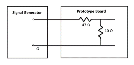
Notice that the input resistance of this divider is $57\,\Omega$ rather than $50\,\Omega$ due to the use of preferred values and that the ratio is 10/57 = 0.175 rather than 0.2. These small discrepancies should be taken into account in the interpretation of your results. Remember to set the generator to ‘Low Z’ which will mean that the voltage appearing across its output terminals will correspond with the readout.
Operational Amplifiers - basics
An Op-Amp is a DC-coupled differential voltage amplifier which is generally shown on circuit diagrams as a triangular circuit symbol. The figure below shows the circuit symbol, the simple generic equivalent circuit for an Op-Amp and the outline of the physical packaged Op-Amp when seen from above. The pin numbers used on the packaged Op-Amp are shown on the circuits diagrams as a value in brackets, eg. the output $V_{o}$ is pin 6:
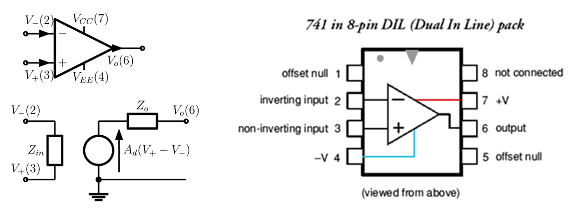
In many circuit diagrams the power supply connections on pins (4) and (7) are omitted. It is assumed that people implementing circuits will know to provide these supplies – otherwise the circuit can not work.
There are many types of Op-Amps and the generic equivalent circuit for the Op-amp is used with different values for $Z_{in}$, $Z_o$ and $A_d$. The Op-Amp has two inputs, the inverting input at pin 2 where the voltage with respect to ground is $V_{-}$ and the non-inverting input at pin 3 where the voltage with respect to ground is $V_{+}$. The output voltage at pin 6 is the product of the differential gain $A_d$ and the difference between the two inputs: $V_{o} = A_{d}\left( V_{+} - \ V_{-} \right)$. For most Op-Amps the currents at the inputs, $i_{-}$ and $i_{+}$, are very small, but finite. With no DC input currents the Op-Amp will not work. Some have an internal bias arrangement so that there is no need for finite DC bias currents to flow into the inputs. The input impedance is often very high, essentially open circuit, while the output impedance is often very low. The differential gain, $A_d$, is often very high and as the output voltage $V_o$ will be a finite voltage between $V_{CC}$ and $V_{EE}$ the difference between the two input voltages is very small, i.e. $\left( V_{+} - \ V_{-} \right) \approx 0$.
Note that the DC supplies needed to power the Op-amp are applied at pins (4) and (7), and that the input (AC) is applied at pin (2) or pin (3). When debugging circuits you should always begin by checking the DC levels in the circuit and the continuity of connections between pins (4), (7) (2) and (3) and the relevant outputs on the power supply and the signal generator. You should perhaps check that the supply voltages are measurable on pins (4) and (7) on the Op-Amp and that ground potential (i.e. half way between the power supply levels) is properly defined. Then look at the DC levels on the signal input pins (2) and (3) and the output pin (6). These should all be at ground potential. If all is well, AC signals should be visible on pin (6) but probably not at the inputs as the levels will be too small.
Amplifier Experiments
For all the experiments ground is the mid-point of the ±15 V power supplies and all voltage measurements (large signal and small signal) are made with respect to ground. The power supply needs to be used in dual supply configuration.
Inverting Amplifier
The circuit schematic for an Op-Amp connected as an inverting amplifier is shown in Figure .
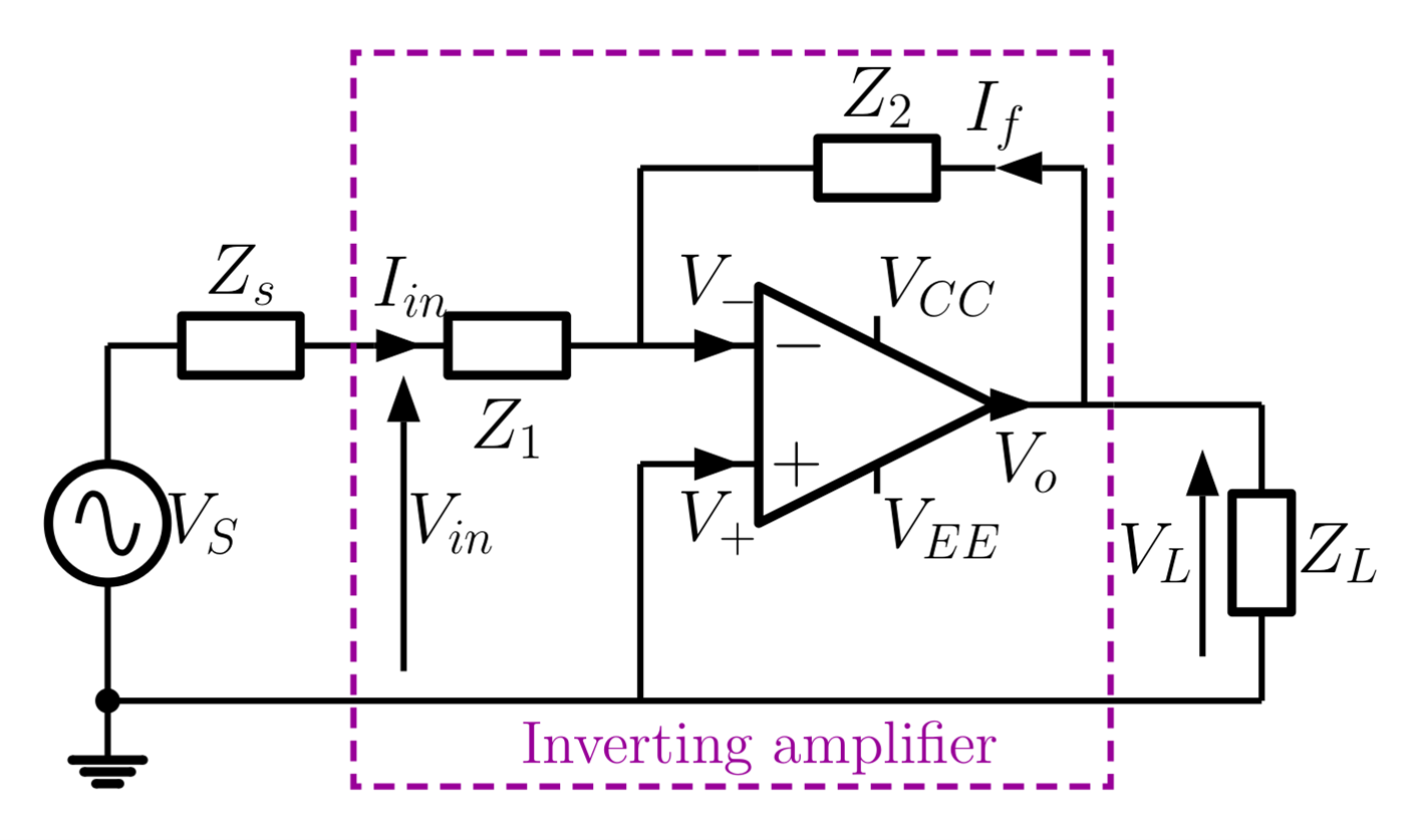
In this experiment the impedances in the circuit will be resistances, so $Z_{1} = R_{1}$ and $Z_{2} = R_{2}$. The closed loop voltage gain $V_L/V_{in}$ of this amplifier is approximately $-\,R_2/R_1$ and it can operate over a wide range of closed loop gains and frequencies. Begin by choosing the resistor values to provide a small signal gain of -10 with an input resistance of $1\,k\Omega$. Use the signal generator potential divider combination to provide an input voltage of 10 mV (pp) at 100 Hz.
Measure the input and output voltages using the oscilloscope and so determine the gain and phase responses as a function of frequency for the amplifier. When making a frequency response measurement you should consider how many frequency points you need and where they should be placed along the frequency axis - should they be equally spaced or grouped in certain bands? More closely spaced measures are needed where the measured response changes rapidly in order to identify that change. Hence taking a relatively coarsely spaced measure across the whole frequency range can identify where the response changes and shows where intermediate measures (i.e. more points) are needed to fill in the detail. The frequency range you can measure over is very broad, 100Hz – 20MHz. Using logarithmically spaced frequencies such as (100Hz, 1kHz, 10kHz…..) or (100Hz, 300Hz, 1kHz, 3kHz, 10kHz…..) for the initial measures is often used.
You will notice that as the frequency is increased, a point is reached at which the gain begins to decline and the phase is no longer exactly 180°. Measure the gain at a range of frequencies from 100 Hz to a frequency well above the value at which the output has fallen to 3 dB below its peak value (or $1/\sqrt{2\,}$ times the peak value). The -3 dB frequency should be carefully noted, it is called the bandwidth (BW) and enables you to calculate the gain bandwidth product (GBWP) for the amplifier, which is an important parameter. Finally, plot gain against frequency and note the rate at which the gain changes at each frequency point. Repeat the experiment for several values of gain (-1000, -100, -1). In summary, this experiment requires you to:
-
Design, construct and test an inverting amplifier with a gain of -10 and an input impedance of $1\,k\Omega$;
-
Measure the gain variation (frequency response) with frequencies from 100 Hz to high values where the gain has fallen well below the -3 dB point;
-
Calculate the bandwidth (BW) and gain bandwidth product (GBWP);
-
Repeat for different values of gain (-1000, -100, -1) keeping the input impedance constant.
When plotting graphs of frequency response please consider the following practical suggestions:
-
Choose the frequency points sensibly-you don’t need many where the gain is ‘flat’, but increase the density where the rate of change is significant;
-
Use log scales for the axes (gain in dB is conventional and you should get used to it);
-
Use normalised gains-i.e. divide all values by the maximum in the set so that max gain becomes 1 (or 0 dB);
-
IN your record of the experiment graphs of data are quite adequate by themselves. Tables of the raw data are best placed in an appendix at the end of your record.
Non-inverting Amplifier
Draw the circuit schematic for a non-inverting amplifier using a single Op-Amp and two resistors. Design and build such an amplifier to provide a voltage gain of 10 and verify its performance at a frequency of 100 Hz. Use the signal generator-potential divider combination to provide a 10 mV (pp) input as for the inverting amplifier. Please note the frequency characteristics of this amplifier will be very similar to the inverting case and so extensive measurements of frequency response, band width etc. are not required.
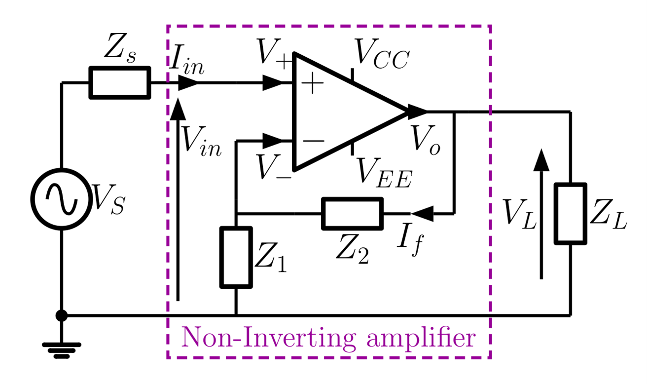
Given an Op-Amp, two $1\,k\Omega$ and two $10\,k\Omega$ resistors, design a non-inverting amplifier with a gain of 10 and an input resistance of $11\,k\Omega$. Build the circuit and verify the gain at 100 Hz. Once again, extensive measurements of frequency response are not required.
Low pass Inverting Amplifier
The inverting amplifier is easily modified to a low pass filter where the corner frequency of the filter can be set by design using the circuit below.
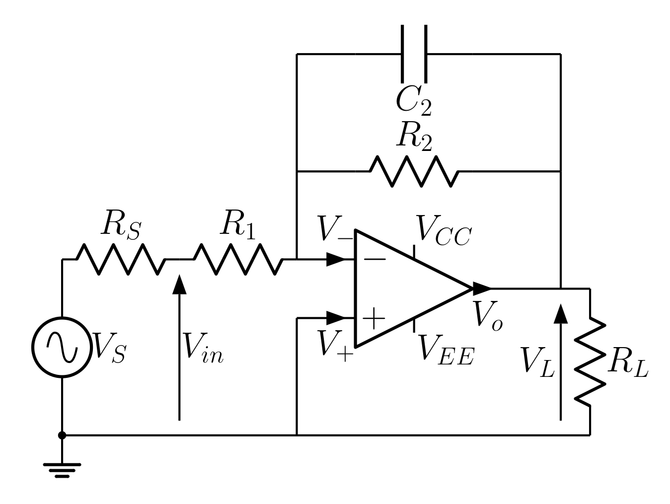
The closed loop voltage gain of the circuit is still $- \frac{Z_{2}}{Z_{1}}$. In this case feedback impedance is $Z_{2} = \ \frac{1}{\frac{1}{R_{2}}\ + \ j\ \omega\ C_{2}} = \ \frac{R_{2}}{1 + j\ \omega\ C_{2}\ R_{2}}$ and the gain is $A_{v} = \ \frac{V_{L}}{V_{\text{in}}} = \frac{- R_{2}/R_{1}}{1 + j\ \omega\ C_{2}\ R_{2}}\ $. The frequency response of the amplifier is then determined by the feedback components rather than the limitations of the Op-Amp.
Connect up the low pass inverting amplifier such that the low frequency input impedance is $1\,k\Omega$, the low frequency small signal gain is $A_{v} = -10$ and the feedback capacitor is 0.8 nF. Measure the gain and phase responses as a function of frequency for the amplifier, and compare the theoretical and measured frequencies where:
-
the magnitude of the gain has dropped by 3 dB from its low frequency value and
-
the phase of the gain has changed by 45 degrees from its low frequency value.