Signal Integrity
Signal Integrity in PCB Design.
Introduction
The printed circuit board (PCB) design skills have creativity aspects that reach perfection over time. We introduce these skills at the very early stage of Electronics and Electrical Engineering programs. This will help students to further their expertise and experiences over the entire program, which will enable them to develop a reliable platform to implement their design ideas in final year projects as well as their future engineering careers. Further to this, due to the top-down educational approach taken in developing material for this unit, utilising a few components that have not been previously studied such as transistors, integrated circuits (ICs), etc, is not a matter of concern.
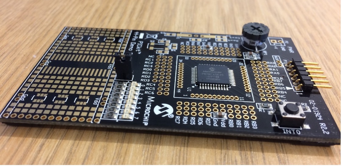
The prerequisites of this project include basic acquaintance with OrCAD circuit schematic (Capture) and PCB design (PCB Editor) environments. The project objective is to initially explore the entire design procedure of a two-layer PCB, which is in this case specifically focused on a test platform for microcontroller circuits. Subsequently you will apply the signal integrity design rules learned in the lectures to your initial layout design. Therefore you will:
- Design a PCB for the supplied schematic circuit and submit the Gerber files ready for manufacturing
- Apply the knowledge of “Design for Signal Integrity” obtained in the lectures to modify your design in OrCAD environment and submit a short descriptive explanation about your approaches
Instruction
Step1: Import the supplied schematic circuit and design the PCB layout
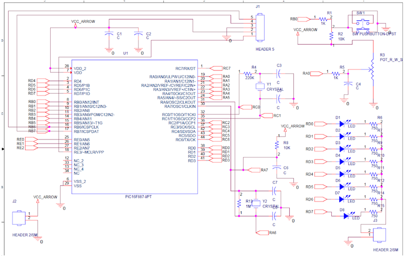
The schematic circuit including the components and connections is shown in . Proceed with the following steps to capture this circuit on your computer.
- Run Capture CIS Lite on your computer
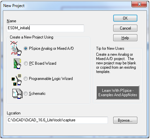
- Create a new project by choosing New from File menu
- Type in a meaningful name in the box shown in for your project such as
ESDM_<initials>, where<initials>is your Bath University username Note: Depending on the computer admin rights you might have to change the Location to a folder on your personal drive - In the next window select create a blank project and press Ok
- Download the ZIP file from the unit Moodle page (Week 2:
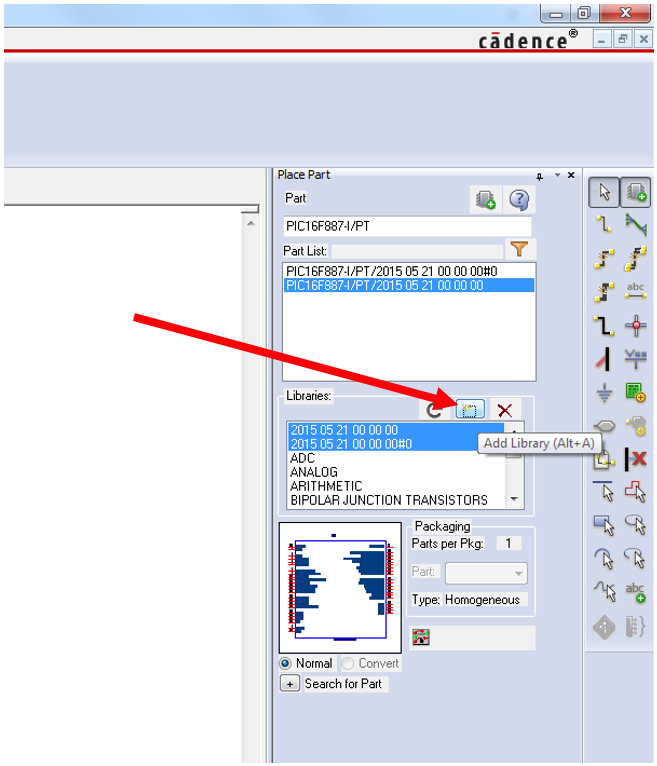
Footprint and Schematic Symbol Library.zip) for the required schematic symbol and footprint libraries. Unzip the file on your personal drive. - Copy 2015 05 21 00 00 00.olb file (microcontroller schematic symbol) and paste it in the schematic library folder:
- C:\Cadence\SPB_17.2\tools\capture\library
- Add the new part library from the folder above to the working library as shown in . In order to do this, click on the radio button shown by the red arrow and select the file that you just copied in the folder above
- This will add the component schematic symbol in the part list
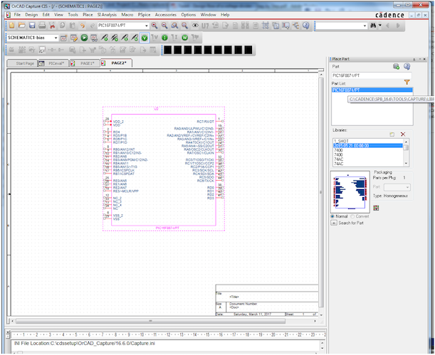
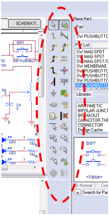
- Place the new component in the schematic window by double clicking on the part in Parts list as shown in
Netlisting is the process of assigning the circuit schematic symbols to their corresponding PCB footprints. Normally the schematic circuit should be netlisted after placing and wiring all components, however, as it is the first Cadence experience we will make sure that the circuit can be netlisted after adding the microcontroller footprint, which is not available in the OrCAD native library. In order to do this:
- Supply the PCB footprint for the microcontroller schematic symbol:
- Copy the .dra, .psm and .pad files from the ZIP file downloaded from Moodle and paste in C:\Cadence\SPB_17.2\share\pcb\pcb_lib\symbols
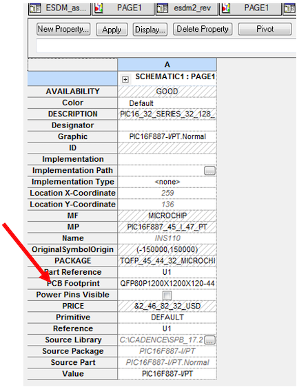
- Double click on the schematic symbol of microcontroller and copy the name of corresponding .dra file (QFP80P1200X1200X120-44N) in the PCB Footprint box as shown in
- Netlist the circuit:
PCB Editor should open a new window where components can be placed to create a PCB.
- From Place menu, select Components Manually…
The microcontroller footprint should appear in the list as shown in .
- Click Hide and place the component on the board by clicking the mouse left button
This confirms that you have nelisted the new component appropriately.
In the next step, find the remaining component schematics and place them on the schematic capture and make the required connections as shown in . Each of the other components in this schematic circuit must be added from corresponding libraries. For example:
- Capacitors, resistors, LEDs, Crystal oscillator and the Pushbutton switch (SW Pushbutton-DPST) could be fetched from Discrete library, while 2-pin and 5-pin connectors from the Connector library
- Symbols such as ground, power supply and ports could be placed from Draw menu, which is on the right hand side of the schematic window in
In order to netlist the supplied schematic circuit diagram, each component needs to have a footprint that matches its pin configuration. For example the microcontroller schematic diagram was introduced by a QFP footprint downloaded from Moodle. Similarly, appropriate footprints must be introduced to the remaining schematic symbols before netlisting the entire schematic.
In order to assure the timely design and manufacture of PCB, we will use the available component footprints.
- Assign the correct footprint to each schematic component as explained in the following
For resistors, capacitors and diodes there are several footprints. In order to handle the tiny component during manual assembly/soldering process we have selected a normal 0805 footprint.
- To modify the component attributes, double click on the component in Capture environment and change the PCB footprint to 0805 for resistors, capacitors and diodes
- Note: this footprint is specifically designed for polarity sensitive components (diodes and some capacitors), however it works perfectly fine for resistors, etc.
- Supply pot for potentiometer footprint
- Supply 7A_XTAL for crystal footprint
- Supply PBSW for push button switch
- Supply jumper2 and jumper5 for two-pin and five-pin header connectors, respectively
Now the circuit is ready for netlisting.
PCB Editor should be closed before netlisting. The procedure above will lead to automatically open PCB Editor where you can see if the components are netlisted appropriately by checking each of them from Place menu.
The board properties, including dimensions, material, etc. needs to be defined in OrCAD PCB Editor. The most straightforward way is to use the wizard.
- Run PCB Editor lite
- Click on the File menu
- Select new and in the drawing type choose Board (wizard) ()
- Supply a name for the board and click Ok. The board file will be created in the following address by default: C:\OrCAD\OrCAD_16.6_Lite\tools\capture\allegro
However, it might be saved on a different location depending on what you have supplied in a.
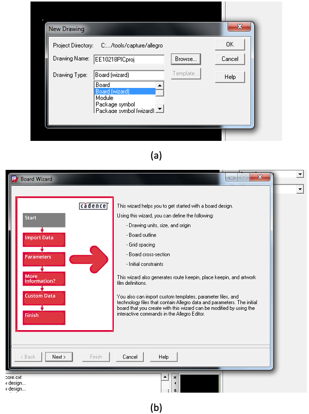
Board Wizard dialogue window provides a way to supply the information needed for the board geometry and other specifications required for board design environment. We don’t have any board template, hence…
- Select No and click Next
Technology file is needed when certain board characteristics are intended. For this project we neither have technology file nor interested in supplying parameters.
We don’t need to import a board symbol at this stage so…
- click Next
In parameters window
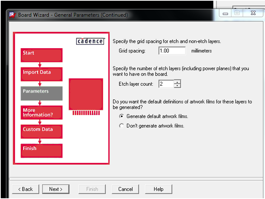
- Set the units to Millimeter and size to A3, then click next
- Leave the grid spacing at 1 mm as it can be altered later
- Here in this dialogue box the number of PCB layers can be set as shown in , which is two layers for the project
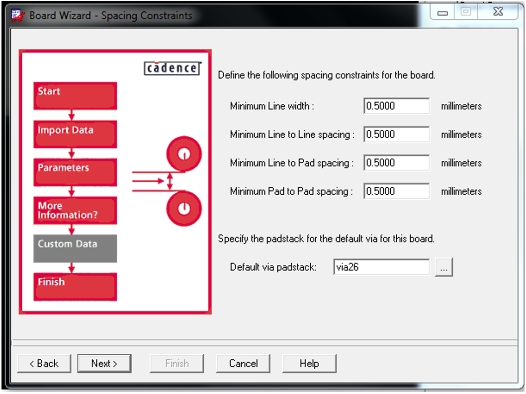
Next the spacing constraints need to be set as shown in . These constraints are determined by signal integrity and circuit performance criteria such as current handling capability, line impedance, etc., though limited by the PCB fabrication technology. It means that how precise the fabrication system can be in etching copper traces, pads etc. For example the CNC machine in the department of Electrical and Electronic Engineering labs is capable of making minimum line width of 20mils.
Another important design criteria is the size and type of via that can be determined in this window.
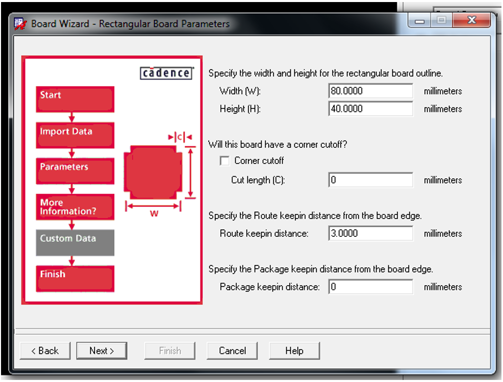
One final step in PCB design is to define the board dimensions. It sets out the board outline, which is needed in the fabrication step to cut the required area from a larger bare board. At this step designers should make a rough estimate of the board size based on the size of the components that can be found in their datasheets.
- Enter 80mm for the length and 40mm for the width that is more than enough for the circuit in this project, however, you might need some extensions to be added to access all ports of microcontroller
- Enter 3mm and 5mm for Route and Package keeping distances. This is the safety margin that avoids the packages and routes to be placed too close to the board edges. If it happens the software generates DRC errors
At this stage, the circuit schematic associated with footprints and bare board is ready to accommodate the components.
- Reopen the project in OrCAD Capture and select (highlight) the schematic file (PAGE1) in the project management window, which was created in the previous step, in the project manager window
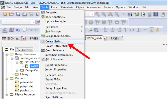
- From menu bar select Tools
- Select Annotate (it assigns dedicated numbers to components)
- From the same menu select Create Netlist
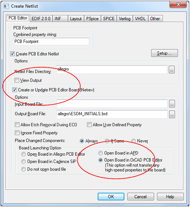
- The dialogue window in will appear
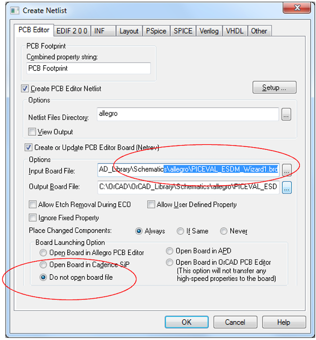
At this stage the predesigned bare board should be introduced to Capture. It can be accomplished by browsing the board file just created in PCB Editor (PICEVAL_ESDM_Wizard in this case) as shown in .
- Browse for the board file that was created in PCB Editor wizard
- Select Do not open board file; later in PCB Editor it is possible to import the netlist on this board
After clicking OK, Netlisting the design and Updating PCB will proceed. PCB editor will not open automatically
- Reopen the board file (.brd file) just created in wizard in PCB Editor Lite
- Its outline should appear but without any components
- From menu bar, select Setup, activate the grid that helps placing components in appropriate position
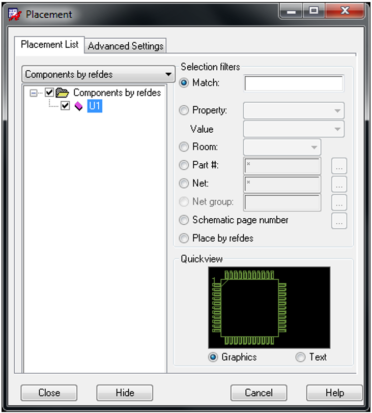
- From Place menu select manual, a window that lists the schematic components appears as shown in
Note: If the list appears with no components, you need to update the netlist from which this board is generated.
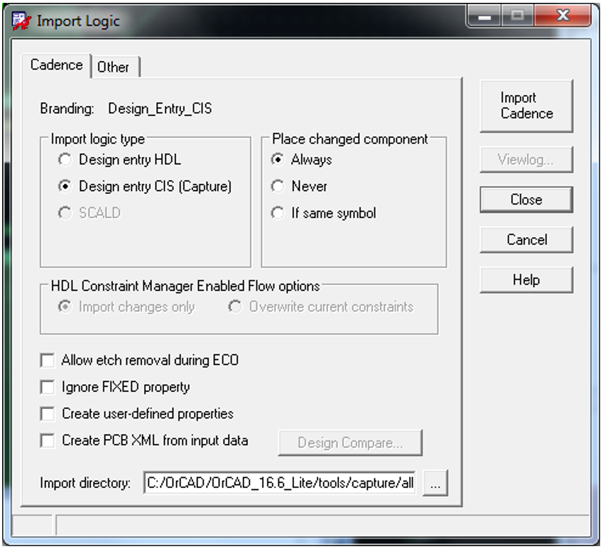
- From File menu select Import and Logic
- The dialogue window shown in appears
- Select CIS (Capture) for design entry type, and browse for the netlist file location that introduced to netlister in Capture: …/algro
- Click on Import Cadence
- Now the component list should appear in Place, Component menu as shown in
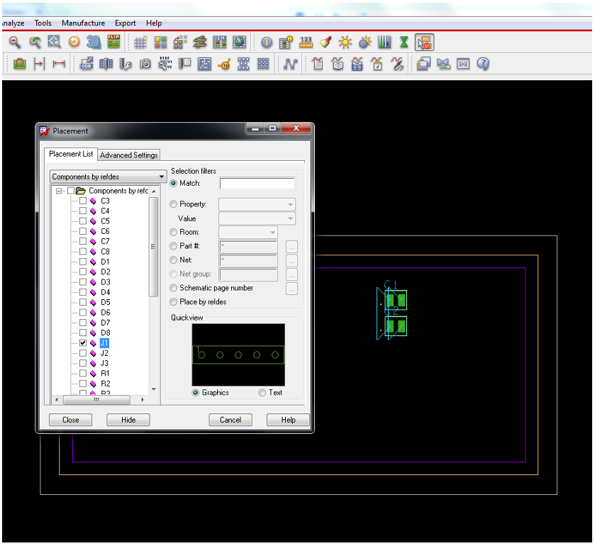
- Select each component and click Hide. The selected component attached to the cursor can be placed on the board by a left click
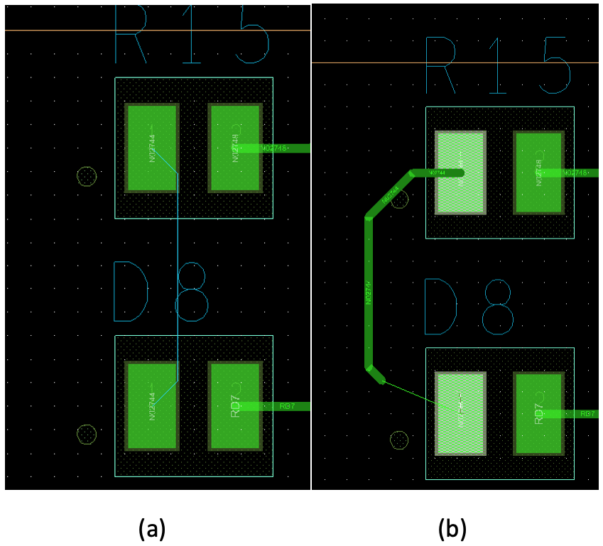
After placing all components in appropriate positions so that they require minimum wire lengths, start routing.
- Use Add Connect (F3) from the menu bar at the left of your PCB editor screen. By clicking on any pad and following on the connection line (natrest) a) the line changes to (thick green) trace (b) that can be terminated by second left click on the destination (second) pad
Vias can be used whenever a trace needs to transfer to the other side of the board for example to jump over another trace (or traces) on one side of a board (obviously without making electrical connections to those ones!).
- After clicking on one pad and starting to route wherever a via is needed click once, then right click and select Add via. Via will be added at that point and routing will be transferred to the bottom layer whose conductor is in a different colour to be recognised from top layer
DRC errors are normal on the first try.
- It is recommended to activate On-Line DRC Check from Setup menu. It helps in locating the error during manual routing
Most of the errors at this stage are due to the default settings on spacing constraints. They are adjustable in constraints setting:
- From Setup menu select Constraints → Spacing
- For example after placing the microcontroller footprint, if you update DRC, red crosses that indicated DRC error appears on its pins. It refers to smd pin to smd pin spacing limit that is set to a higher value than its actual value
- From Constraints → Spacing in the table find smd pin to smd pin and change the default value to a lower than actual value such as .1mm
- Close the constraints window
- By updating DRC the errors (red crosses) disappear
- Special care should be taken to avoid violation of fabrication limits. For example, if you use the department CNC machine to make your board, minimum line width is 20mils
- Use Text from Add menu to write your name (initials) in the etch layer on board. This will help distinguish your board among the others after being delivered from manufacturing company
- Save a copy of your board file that is free of any DRC errors and approve it by your supervisor
Final stage in PCB design is to send your design files for manufacturing. Manufacturing company generally does not need information about operation or application of our boards. They make copper traces at the top and bottom of a board and drill holes for through-hole devices and metal-plate the holes wherever it is needed. Therefore the size of the board (Outline), mapping of traces and vias (top and bottom) and drill holes (NC Drill) need to be supplied to the manufacturing company.
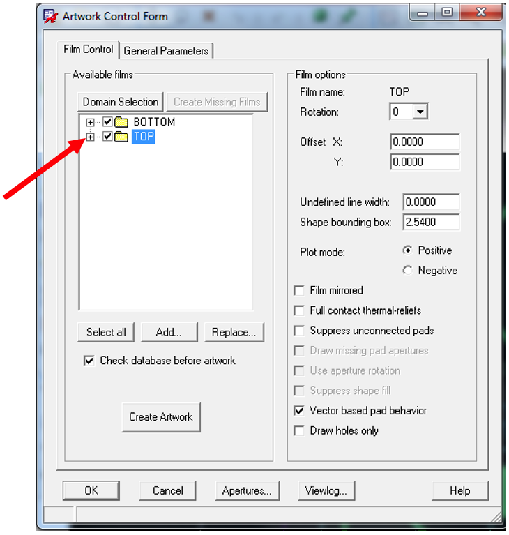
- From Export menu in PCB Editor select Gerber that can generate the mapping of pads, traces and vias separately for bottom and top layer by default ()
In addition, the board outline needs to be added in the artwork list. However the thickness of outline needs to be adjusted first. By default its thickness is zero, which makes it invisible to artwork.
- Right-click on outline and select change width. Enter any value in the range of .2mm in the dialogue box and click Ok
The easiest way to include outline in the artwork list is:
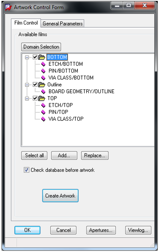
- To right-click on TOP folder in Artwork Control form () and select Copy
- This create a new folder where you can change its name to Outline by left click on the folder name
- Click on the + sign as shown in to extend the folder and right click on the components and select Add
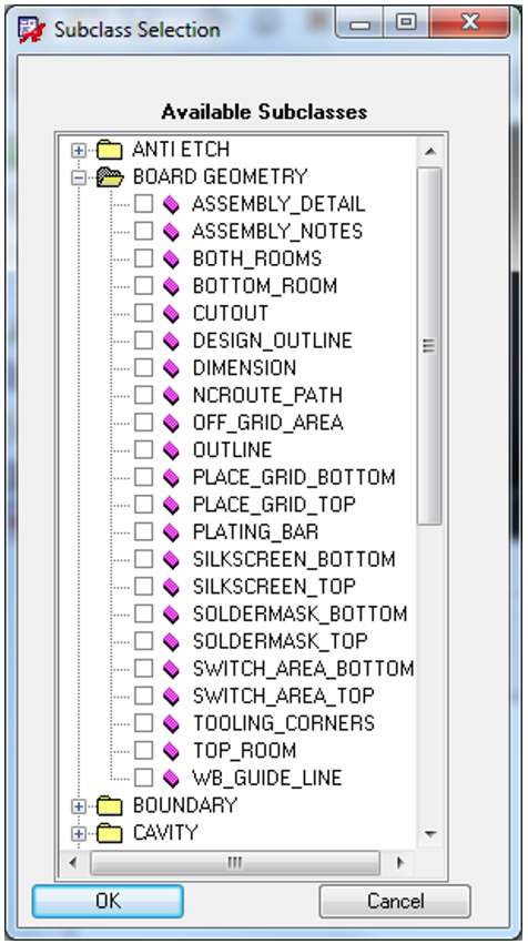
- It opens a new window as shown in , where you select Board Geometry and tick outline and click Ok
Now the artwork dialogue window should look like .
- Make sure in the General Parameters tab select Gerber RS274D which is understandable for most of manufacturers
- Click on Create Artwork
Two files will be generated with .art extensions in the following location on your disk:
C:\OrCAD\OrCAD_Library\Schematics\allegro
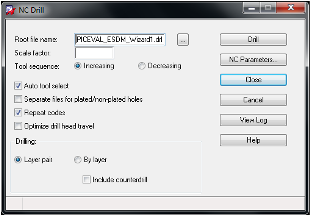
In order to generate the coordinates and properties of holes to be drilled on the board:
- From Export menu select NC Drill, the dialogue window in appears
- By clicking on Drill it will generate a file with .drl extension
- Pay attention to the location of .drl file on your hard disk. It will be needed later when you check the validity of the file on Gerber Viewer as well as sending the .drl file to manufacturers
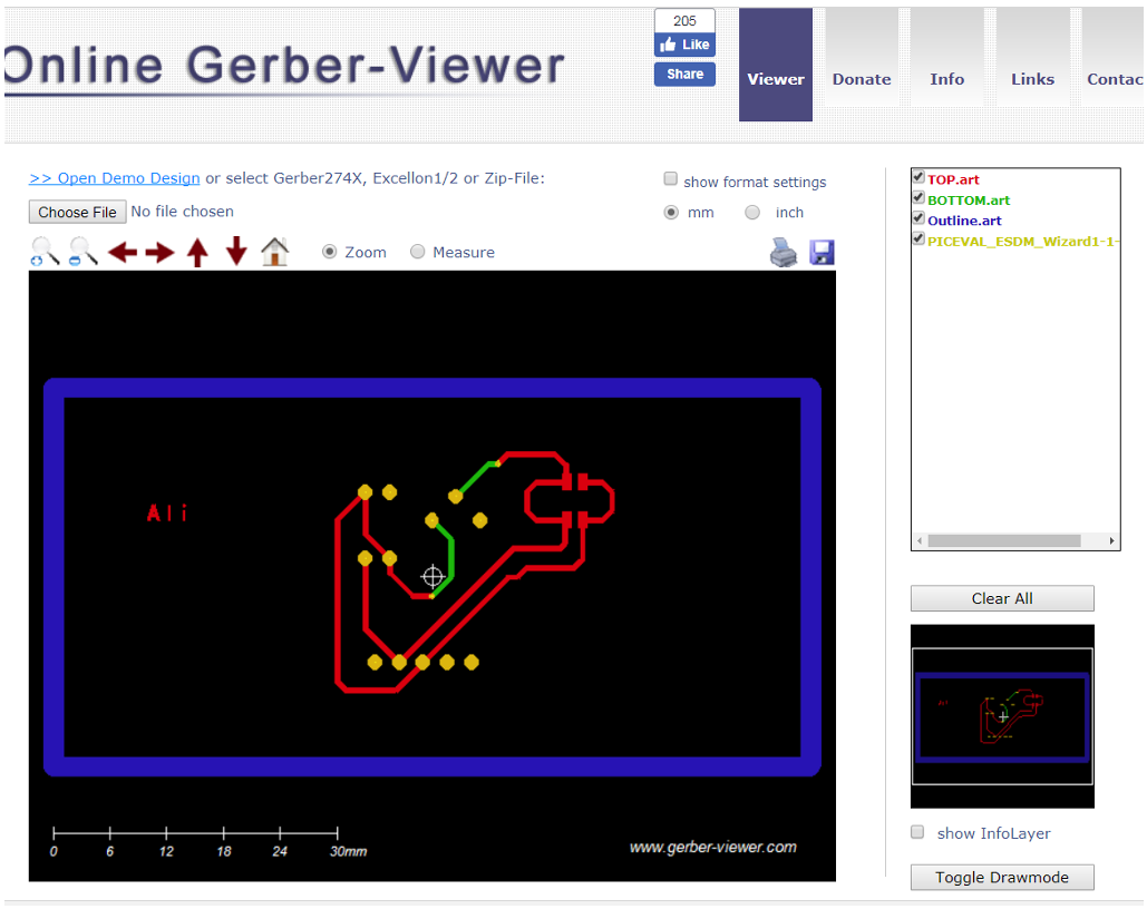
In order to check the validity of your artworks for manufacturing process use online Gerber viewers to see your files (.art, .drl).
- Using a web browser of your choice, go to Gerber Viewer
- Browse your files and check them with your supervisor
- Make a ZIP file that contains the four files and submit it to Moodle
With reference to your lecture notes and texts on Design for Signal Integrity, revise the initial layout (redesign the PCB layout) and apply the signal integrity rules you learned in the lectures. For example, comment on how you could change the design in order to make it less vulnerable to electromagnetic interferences. You might have already considered these principles in your initial design. In this case you could comment on what rules you have already applied.
Copy and paste screenshots of the initial layout and revised layout to your report and compare them by highlighting the changes (at least three cases) on the figures. Use a graphical editor such as Microsoft Paint to add arrows, circles, etc, to highlighting the changes.