Thermal Design 1
PCB Design for Thermal Considerations.
Introduction
This lab manual introduces a few PCB design techniques for improving the heat dissipation from the electrical/electronic components to the board and then to the ambient, which keep the entire system within safe operating temperature limits. Students will apply these techniques and the knowledge obtained in lectures to redesign a PCB for an example electronic system (DC-DC Converter), and then draft and submit a report on Moodle. Therefore the following learning outcomes are expected from this lab session:
- Practice the footprint library design for power transistor
- Add heat spreader copper layer on PCB
- Add thermal vias
- Draw PCB layout for the DC-DC Converter
- Redesign the board layout to improve the heat transfer
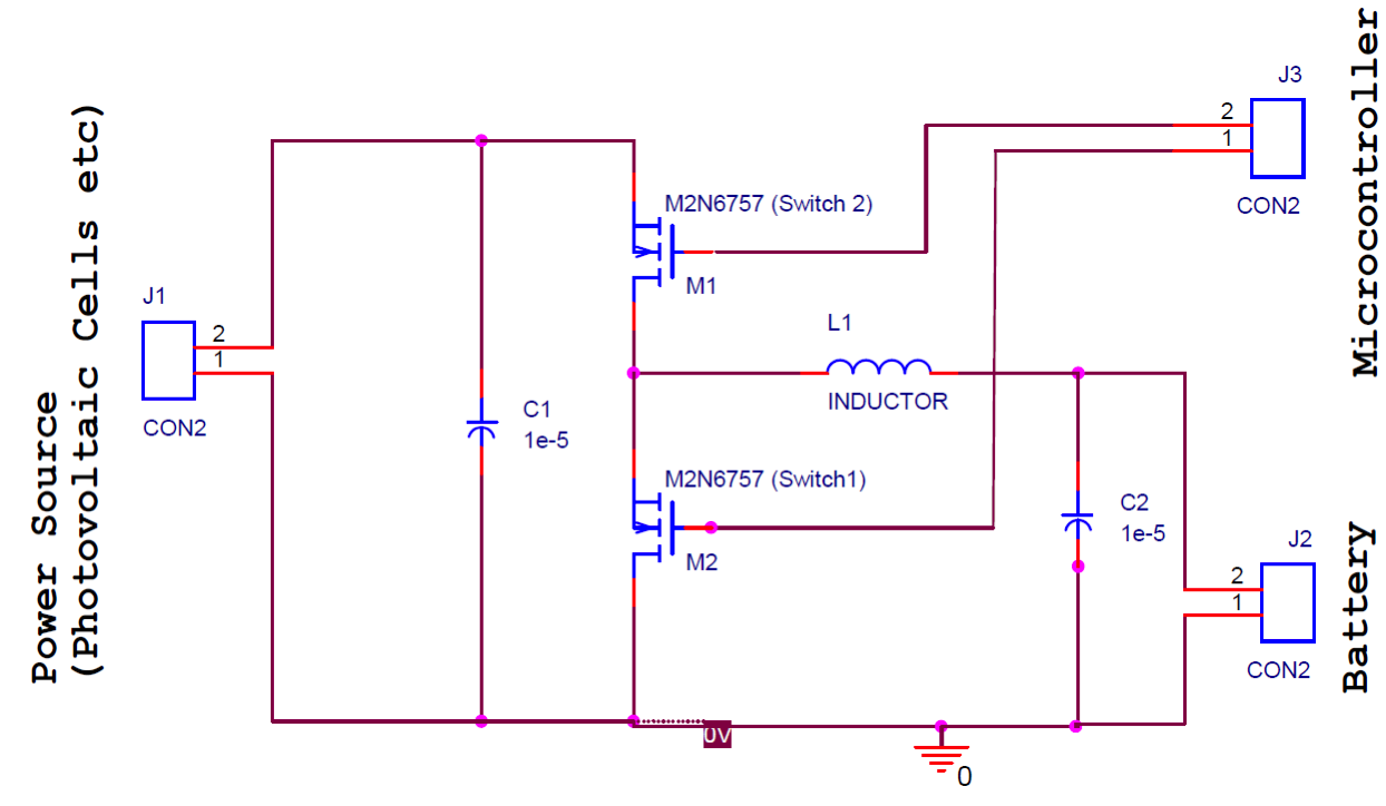
DC-DC Converters; An Example Hot Spot on PCBs
The DC voltages generated by different electrical energy sources or power converters is not essentially equal to the voltage level required for supplying power to the load. For example, the desktop computer power supply units generate 12Vdc from the ac input, while on different boards such as graphic cards, main boards, network adapter, etc. there are chipsets that operate only with 3.3Vdc or 5Vdc etc. Therefor the dc voltage need to be reduced while the required current might even increase. Another example is the photovoltaic cells that generate a voltage level much higher than the nominal voltage of batteries. Hence the generated voltage level must step down while a higher current is needed to charge the batteries.
DC-DC converters are electronic switching circuits that adjust the dc voltage of source before delivering power to the load. illustrates an example DC-DC converter that is designed to supply power from photovoltaic cells to a load and charge batteries. The load is omitted here for simplicity. The two transistors operate as switching elements to conduct certain level of power (voltage*current) to the loads.
Conducting current through a resistive element in any electrical/electronic component can increase the temperature, which is proportional to the level of electrical power. The transistors temperature could increase for two reasons:
- Conducting high levels of power from load to source, which is very common in power electronic circuits
- Switching at high frequencies that lead to an on/off short circuit between rail voltages (supply and ground)
These two are unavoidable in many circumstances. Hence the designers must…
- Choose appropriate components with minimum thermal resistance
- Apply PCB design techniques to use the copper on PCB for cooling the hot spots
- Use heatsinks or forced air (fan)
taken from: V. Viswanatha, R. Reddy, “Microcontroller based bidirectional buck–boost converter for photo-voltaic power plant”, Journal of Electrical Systems and Information Technology, June 2017.
Design Steps
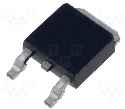
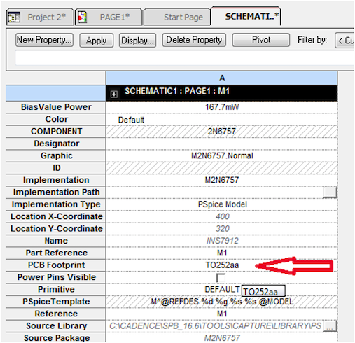
Draw the schematic in using OrCAD Capture. If you don’t have the transistor library on your computer it is possible to use other transistors. (This transistor is available in pwrmos library). We will not simulate the circuit at this stage. However, you will need to choose appropriate footprints for your transistors. One example footprint option for the transistor in this application is TO252aa, which is shown in . In your reports you need to explain the criteria based on which you have chosen any alternative components or modified the footprint.
- Make sure all other components have appropriate footprints, for example ck17-10pf for capacitors and ax1000x225034 for the inductor
- Netlist the circuit
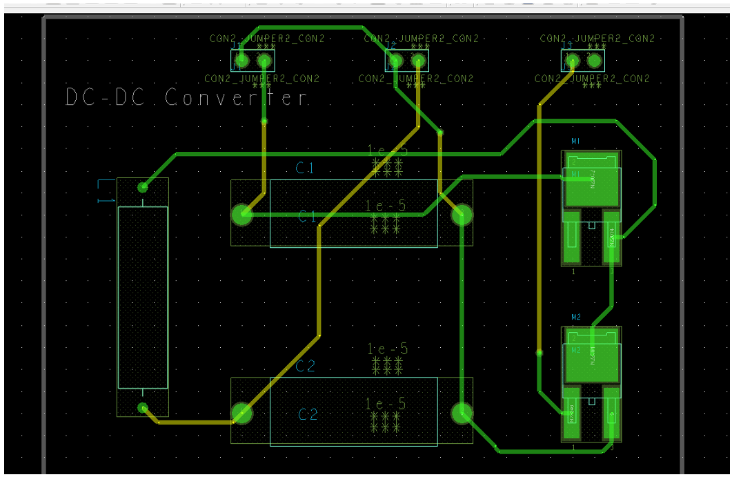
- Place the components and rout the layout in PCB Editor environment
- Save a copy for your reports
Thermal Vias and Heat Spreaders
There are several methods to reduce thermal resistance of the path from case/packaging of electronic components to the ambient environment (ƟCA). One way is to add thermal pads underneath the components with an exposed pad and transfer the heat generated by component through thermal vias to the bottom side of the board, which is a copper plane as shown in .
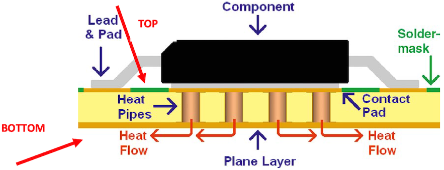
There are a number of PCB design techniques to achieve an efficient thermal structure. In this experiment you will practice the design of:
- A: Footprint for transistors with exposed pads
- B: Thermal vias
- C: Heat spreaders
…and how to use thermal vias to connect exposed pad to the bottom layer of the board.
Part A: Design a Footprint for TO252 Transistor Package
Reminder: You learned there are two steps in creating footprints:
- Use Padstack Editor to design pads based on the size and geometry information provided in the datasheet
- Use PCB Editor Lite to:
- Place the pads according to the topology provided in the datasheet
- Draw a Package outline
- Assign a reference designator (RefDes)
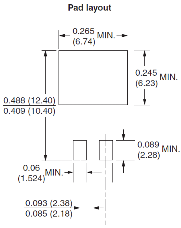
The transistor pad layout is shown in , which is taken from its datasheet.
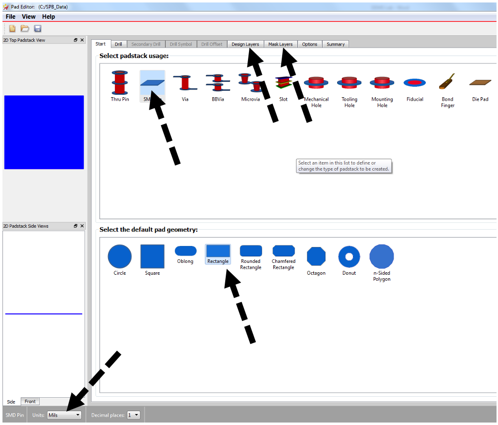
- Run Padstack Editor on your computer ()
- Set the units to mils
- Select Smd pin and Rectangle as padstack usage and default geometry respectively
- Switch to Design layer tab and enter the width and height of the pad according to
- Width = 265mils, Height = 245mils
- Switch to Mask Layers tab and select Solder Mask Top
- Select Rectangle as its geometry and add 10 mils to width and height of the pad above, hence:
- Width = 275mils, Height = 255mils
- From File menu save this padstack in Symbols folder (following address) as TO252AA_D
C:\Cadence\SPB_17.2\share\pcb\pcb_lib\symbols - Repeat these steps to make source/gate pads (smaller pads in ) and save it as TO252AA_S_G in Symbols folder.
Now pads are ready to be placed according to the datasheet topology in PCB Editor to create the footprint.
- Run PCB Editor Lite on your computer
- From File menu select New
- In the new dialogue window enter a name (TO252AA) for footprint and select Package Symbol
- From Layout menu select Pins
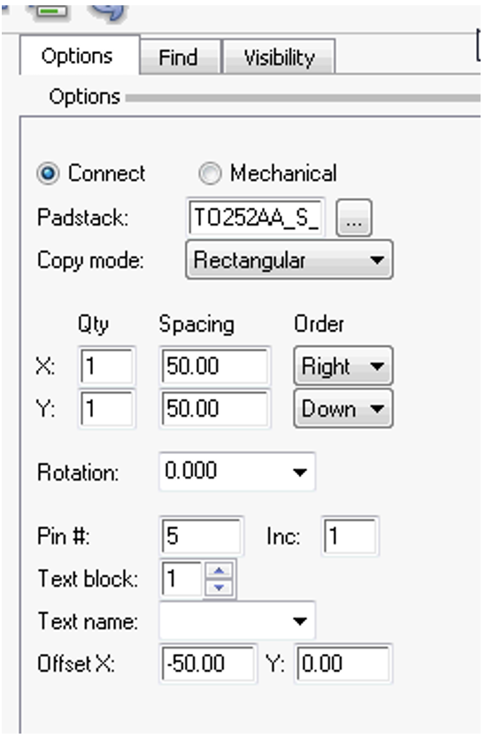
- Choose the pads created above from Options pane as shown in
- Place the pads as close as possible to the page origin (Coordinate: 0,0) as shown in
- Use Add line tool to draw the package outline while the Package Geometry class and Place_Bound_Top subclass is selected in Options pane, as shown in
- From layout menu select labels and select Refdes
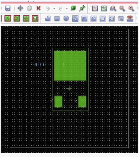
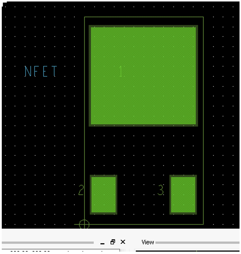
- Left Click somewhere near to the footprint and type in a Reference Designator such as NFET, as shown in
- This RefDes should match the one used to describe schematic symbol if needed
- Save the created footprint as
TO252AA_<Your_initials>in Symbols folder
The footprint is now created.
Part B: Thermal Vias
In order to create thermal vias you can use Padstack Editor. Thermal vias are structured like normal vias.
- Run Padstack Editor
- Select via and Circle as the usage and geometry, respectively
- Switch to Drill tab
- For Hole type select Circle
- For Diameter, enter 30 mils
- For Hole plating select Plated
- Switch to Design Layers tab
- Since the target board is a two layer one, therefore you only need to define Begin Layer and End Layer
- For Begin Layer, Select Circle Geometry and enter 20 mils for diameter
- Copy the Begin layer and paste it in End layer
- Save the via as
VIAHEAT.pad - Close the warnings window and click Yes to save
The design of thermal vias are finished now, however, in order to set them as the default via we might either apply some changes to Constraint Manager settings while the boards are being laid out or use Board Wizard to create the new board and set the default via padstack. We took the second approach in this experiment.
Part C: Heat Spreader and Placing Thermal Vias on the Transistor Footprint
You have two options for this part of experiment:
- Use the footprint created in part A and proceed
- If you have skipped part A you can use TO255AA.dra from Symbols folder
Create a new board:
- Run PCB Editor
- From File menu select New
- In the dialogue box enter a name and select Board Wizard
- Proceed with wizard until the dialogue window called Spacing Constraints appears
- Enter 20 mils for each constraint
- Find and select viaheat.pad in Symbols folder as the default via padstack
- In the next window select Rectangular shape for the board with 1000mil*1000mil size
- Finish the board wizard
- From Place menu select Component Manually
- In the Placement window switch to Advanced Settings tab
- Select Library tick box
- Switch back to Placement List and from dropdown menu select Package Symbol
- Find TO252AA_Initials in the list and select its tick box
- Click hide and place the transistor on the canvas as shown in
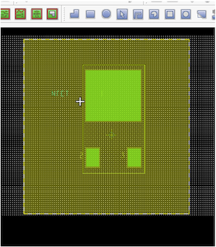
- Draw a rectangular on the board as shown in , while class Etch and Subclass Bottom is activated. This is the heat spreader, which is indeed the copper at the bottom of the board
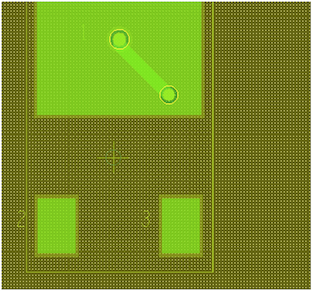
- Now place thermal vias to connect the transistor drain (large pad) to the heat spreader
- Use add Connect tool for this purpose and click on the drain pad
- Right click and select Add via
- On Options plane the via type should be VIAHEAT
- Repeat the last step as many times as vias are needed to make a low thermal resistance, shows adding two vias
- Generate a 3D image using 3D tool in the tool bar
- From view menu select Hide Component and z-scale the image by 10