Multilayer in OrCAD
High-density Component and Multilayer Board Design.
Introduction
In the last lab experiment, footprint design for components with custom footprints was introduced. However, most of the IC (integrated circuit) packages follow a geometric standard for compatibility of manufacturing processes. For example the soic8 footprint that you used for netlisting the schematic circuit of the OpAmp is a commonly used footprint for many other IC packages. In this lab session, the inbuilt module for creating an advanced package footprint will be introduced first. Then you will apply required changes to assure it fully and correctly represents your specific package as described in the datasheet.
In the second part of this lab you will practice the design of multiplayer boards (MLB) as introduced in the lecture. To make a one-to-one comparison, you will practice the multilayer implementation of the two layer board you designed for the amplifier circuit in the first session.
1. Footprint Design for an Example Pin Grid Array (PGA) Package
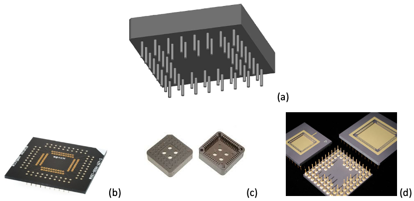
(a) shows the bottom view of generic PGAs, which could be realised in different components as in (b)(c)(d). For example package (d) is especially useful for prototyping purposes where designers have just received their dies from microfabrication foundries. For test purposes they glue the die substrate inside these packages (also called chip/die holders) and use wire-bonding machines to connect the metal pads on the die to the package pads for providing electrical access to the die through PGA pins and to the PCB. Depending on the size of die and number of required pins there are several PGA packages.
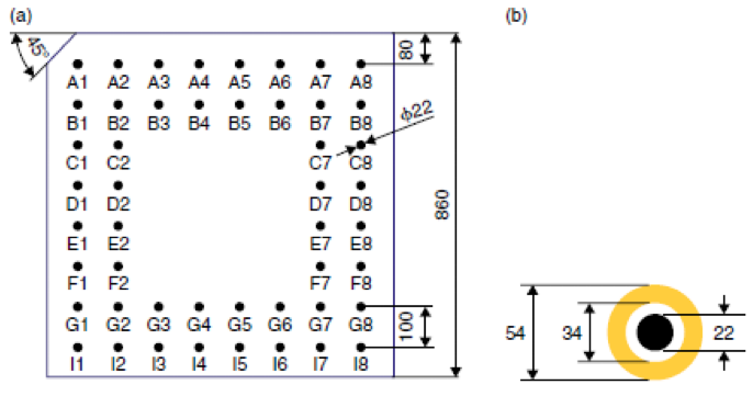
We consider a 48-pin PGA package as an example to practice generating footprint library. The component datasheet for these packages supply the pin configuration/distances and size of each pin (all in mils as shown in ), in addition to other useful information.
The inbuilt module in PCB Editor generates footprint library for common package types.
- Run PCB Editor Lite
- From File menu select New
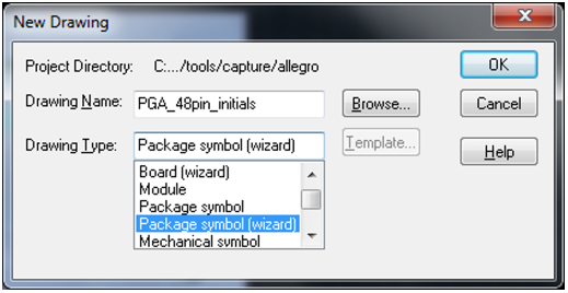
- A new dialogue box as shown in appears, where you should choose New Package Wizard as the Drawing type
- Supply a file name in the dialog box such as
PGA_48pins_<initials>(where<initials>is your Bath University username) and click Ok
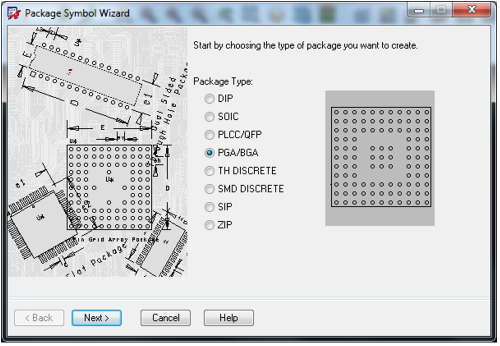
- Select the package type (PGA) in the next window as shown in and click Next.
- By clicking on other package types such as DIP, SOIC, etc. you could review the packages that were introduced in the previous lectures.
- Note: OrCAD uses similar topologies for BGA and PGA packages, however, their pin type is different. In the following steps the pin configuration of package will be explained where the two packages are differentiated.
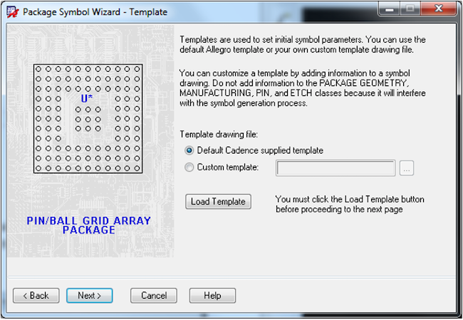
- At the Template dialog box (), leave the Default Cadence supplied template radio button selected and click the Load Template button. At this stage the grid appears on the layout page.
- Click Next.
- For the General Parameters dialog box, leave the default settings (mils) and click Next
- Pay attention to the default reference designator (U*), which is a mandatory part of footprint and could be used to create the corresponding schematic symbol for netlisting from schematic to PCB layout.
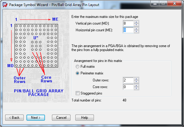
In the next dialogue box (), pin layout of the package is determined. It is derived from the datasheet in .
- Enter 8, for both vertical and horizontal pin counts
- Enter 2 and 0 for Outer and core rows respectively
- Note: This package is not a full matrix
- Note: Total number of pins is 48
- Click Next
In the following window you will have the option to choose the pin numbering format.
- Choose Number Horizontally and click Next
- Note: this option is chosen to simplify the testing of footprint validity while assigning to schematics
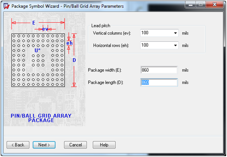
Leads pitch and package length/width, provided in datasheet, are supplied in the next window.
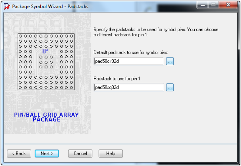
The difference between PGA and BGA packages is determined at the following stage where the padstacks should be selected. These padstacks can be created by the designer using Padstack Editor. However, we will use the padstacks available in the native library.
- pad50cir32d for the default padstack and pad50sq32d for the pin 1 padstack as shown in . A different pad for pin number 1 helps in placing the component in the manufacturing process
- Click Next
The resulting footprint is shown in .
- Save this footprint in symbols folder and check that PGA-48pin files with .dra and .psm extensions exist in the same folder
In the next step of this experiment the validity of the designed footprint, with regard to netlisting, will be checked.
- Run Capture CIS
- Make a new schematic library for a package with 48 pins
- Reminder from Lab-7:
- Select New from File menu and then select library
- In the project manager window right click on the new library and select New Part
- In the dialogue box enter a meaningful name such as
PGA48-<initials>and click Ok - In the new library window that allows drawing a new schematic diagram, enlarge the default square outline so that 48 pins can fit in its pyramid
- From Add menu select pin and start by pin name (1) and Pin number (1) and populate 48 pins corresponding to the name and numbers of footprint in . The schematic symbol should appear as shown in
- Note that pin numbers are in correct order up to pin 18 and after that is pin 23…
- Reminder from Lab-7:
- Save it and take note of its location on your hard-drive
- Start a new project from File menu in Capture CIS
- In the schematic window, add the schematic symbol of 48-pin PGA package and connect two of its random pins to each other with the wire tool ()
- In order to set the PCB footprint of this component double click on the component and in the PCB footprint box enter
PGA_48pins_<initials> - Save the schematic diagram
- Note: Confirm the one-to-one correspondence between the pin numbers in schematic and footprint library by opening the
PGA_48pins_<initials>.drafile in PCB editor.
- Note: Confirm the one-to-one correspondence between the pin numbers in schematic and footprint library by opening the
- Netlist the circuit, which in this case consists of one component with some of its pins wired to each other (Select Annotate and Create Netlist from tools menu while Page is highlighted in project manager window)
- Setup the create netlist dialogue box so that it opens PCB Editor automatically
- Place the component and check if its pins are connected by ratsnest
- Approve the result by your lab demonstrator
- Submit the .dra, .psm and .olb files on Moodle
2. Multilayer Board Design
In the review lab session an amplifier circuit was net-listed on a double layer board. In this experiment the same circuit will be designed on a multilayer board.
The first step to solve this design problem, after net-listing, is to determine the number and stack-up of required layers, which then leads to setup these layers in PCB Editor.
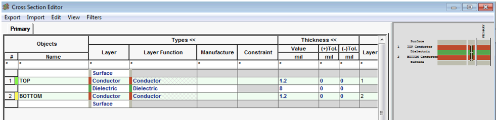
Op-Amp requires two power supplies (V+ and V-), hence two power planes are needed. In addition, one plane is needed for the ground. Regardless of multi-layer board design requirements, for routing the signal traces minimum, two layers is required to connect the components without using jumpers. Therefore, five layers are required to improve the signal integrity of the circuit. However, the multilayer board are usually manufactured with even number of layers. Hence, we opt for a six-layer board.
OrCAD PCB Editor is used to define the stack-up of the board, which determines the sequence of different layers and some attributes associated with each layer.
- Draw the schematic diagram in Figure 3 (review lab: session 1) with an appropriate 8-pin OpAmp, or open the schematic diagram if you have saved it previously
- Check if all of the components are assigned with an appropriate PCB footprint in accordance with Table 1
- Netlist the circuit and adjust netlisting to automatically open PCB Editor. Do not place the components yet
The desired layer stack-up for the board is illustrated in , where two supply planes are sandwiched between two ground planes (Shielded). This stack-up guards the supply line against external electromagnetic interference (Relevant signal integrity topics will be discussed in Electronic Systems Design and manufacture 2 (EE20222)). The top and bottom layers serve as signal routing layers as it was in the two-layer board. A cross-section viewer module is built in PCB Editor in order to manipulate the board stack-up

- Select the cross-section tool from menu bar in PCB editor (). The dialogue window shown in will appear, that shows the available layers in the default stack-up
- Note: The cross-section tool is also accessible from Setup menu.
- In this example we keep the default properties of board geometry and material, however these are adjustable in this dialogue window.
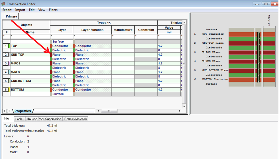
- Right-click on the available TOP layer and select Add Layer Pair Below from the pop up menu in order to define the required layers shown in
- Repeat this procedure four times to have a total of six conductive layers including TOP and BOTTOM
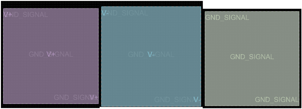
- Double click on the name box of the four new layers and rename them as shown in , i.e. GND_TOP, VPOS, VNEG and GND_BOTTOM
- Note: on the right side of this window there is an image corresponding to the cross section view of the board layers
- In Layer column, change the type of four new layers to Plane by clicking on the corresponding box and selecting plane as illustrated by arrow in
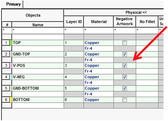
- Click set the Negative Artwork in Physical settings column as shown in . This allows thermal reliefs to be seen in the next steps
- Click Ok
- Note: this stack-up consists of six layers including top and bottom as well as four plane layers. This can be seen by clicking on visibility pane on the right side of PCB Editor
In order to make working with layers while the planes are visible it is more convenient to change the colours of planes to some light colours.
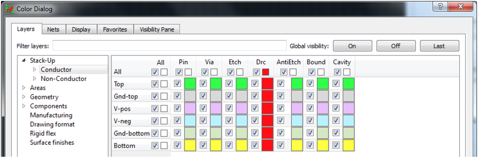
- Select the colour tool () from tool bar. The colour setting dialogue appears as shown in
- Click on Stack-Up

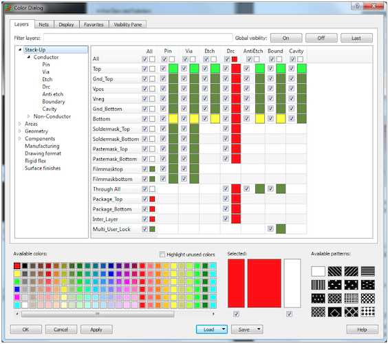
- In order to change the colour of plane layers, click on the available colours at the bottom. The selected colour will be shown on the right side of available colours pane
- Then click on the desired plane
- In PCB Editor, check the grids is activated. (Setup → Grids)
- Select Shape Add Rect tool () from the tool bar
- In Options pane select Etch as active class and Gnd-top as active subclass as shown in

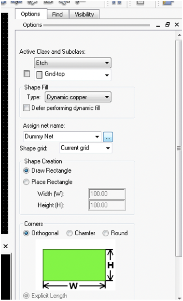
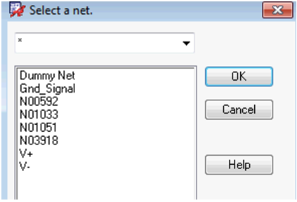
Now we need to assign a valid net name to the plane. Nets are translated from schematic after netlisting.
- Click on the radio button in front of Dummy Net () that opens a list of nets as shown in and select Gnd_Signal
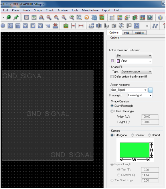
- Draw a rectangle from coordinate (2000, 2000) to coordinate (4000, 4000)
Now Gnd-Top plane layer is built in the stack up as shown in .
- Repeat the same instruction for the other three planes.
- For each plane layer select appropriate subclass and assign appropriate net name.
At the end of each step you should see the following images as shown in .
Now the board is ready to place the component footprints on. However, some of the through-hole pins might need modifications that should be carried out using Padstack Editor tool, which is built in PCB Editor.
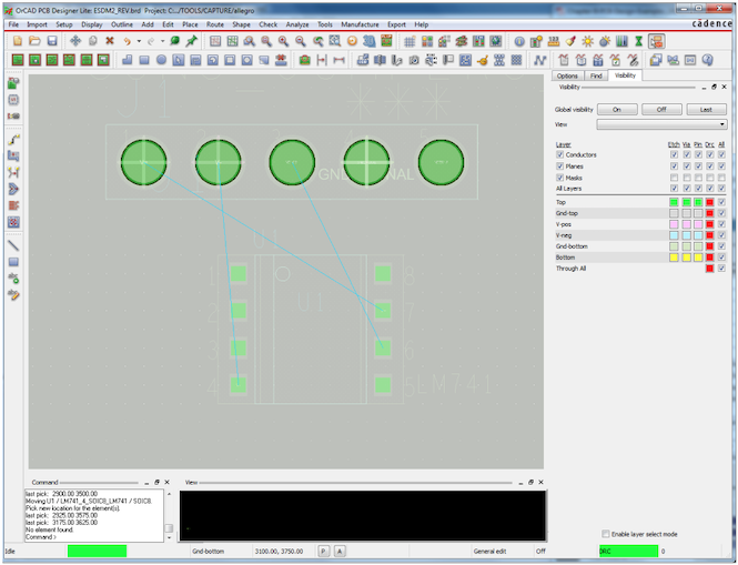
- From Place menu in PCB Editor select Components Manually…
- Choose the 5-pin connector (J1) and Op-Amp (U1) from the list and click Hide
- Use the mouse cursor to place the two components on the board as shown in
If you don’t see cross hairs on pins 1, 2 and 4 of 5-pin connector, it means that either your schematic connections are not made appropriately, or you need to change the layer visibility for plane layers.
- Use routing tool to only connect the connections from 5-pin connector to U1
- Use the 3D tool in the tool bar to generate a three-dimensional image of the board
- From View menu in Allegro 3D viewer tool select Hide Components
- From the same menu select Z scale and enter 10 to see a better view of cross section
- Submit the .brd file generated for multilayer board on Moodle
Design Skills - Coursework
The following questions assess your knowledge of creating footprints and schematic symbols required for the design of multi-layer PCBs. This is a conceptual review of material you learned in Design for Manufacturing, which is a prerequisite for more advanced material in Design for Signal Integrity and Thermal Design.
For recording the schematic symbols, footprints, PCB layout, etc. provide clear image of requested items.
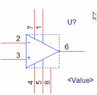
Question 1: Create Schematic Symbol for an Op-Amp
Create a schematic symbol library for the Op-Amp shown in . The pin types should appear appropriately in the circuit diagram that you will draw in the next step (eg. Input, Output, Supply etc.). Name the component with your initials. Therefore instead of U? in , it should appear as U_<your-initials>?.
- Draw a schematic circuit in Capture that includes the Op-Amp only
- Assign a corresponding PCB footprint from the native library (such as soic8)
- Netlist the circuit and place the component in PCB Editor
- Submit the library file (.olb) for the Op-Amp schematic only in Moodle. In your report, describe the procedure to create this symbol, create schematic circuit and netlist. If you couldn’t netlist the schematic circuit, explain the possible reasons in the report
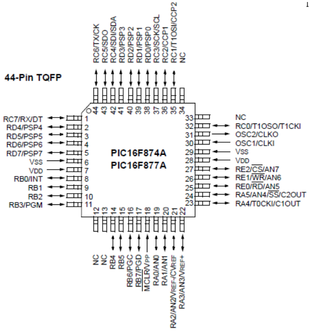
Question 2: Create Schematic Symbol and Footprint Libraries for a QFP Microcontroller
shows the pin configuration and schematic symbol of a QFP microcontroller (PIC16F874A).
- Create a schematic symbol library for this component
- Name the schematic symbol as
QFP_<your-initials>- Reminder: Pin numbers of the schematic symbol must match the corresponding pin numbers of the footprint in the next step
- In order to save your time, name the pins by the same numbers only. For example instead of RC6/TX/CK for pin number 44, just use 44 as the name of the pin, i.e. pin names and numbers can be identical for simplicity
- Write down the folder address where you save the schematic library. While designing the schematic diagrams, component libraries should be added from that folder in the next step
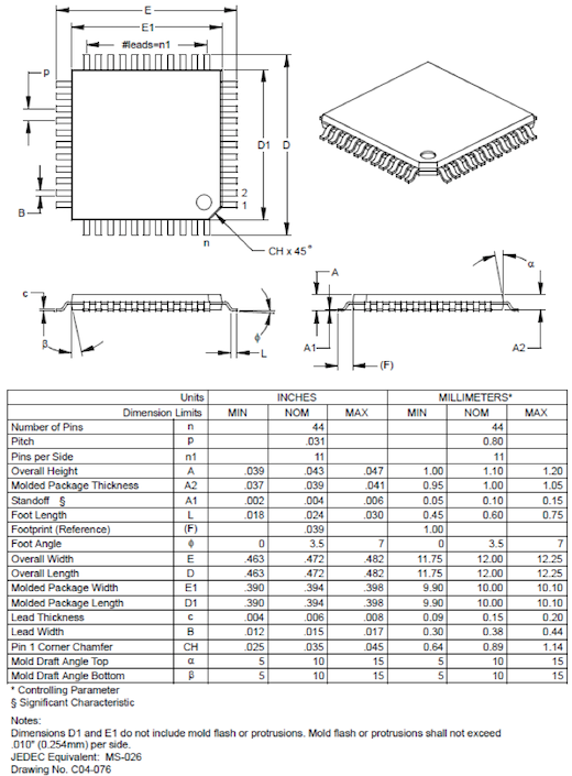
- Create a footprint for this microcontroller that matches the schematic symbol in the previous step. shows the datasheet snapshot for the footprint of a QFP package for the PIC microcontroller
- The required dimensions are listed in
- For the pads these dimensions include the Foot Length (L) and Lead width (B). Students should either design the required pads using Padstack Editor tool or find a native padstack with similar dimensions (if not identical) from available OrCAD symbols library
- For the package these dimensions include Overall width/length (L, E) and Pitch (p)
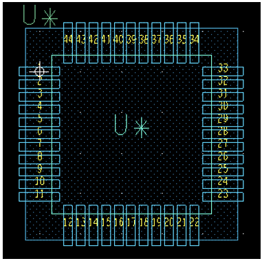
- Regardless of using Wizard or manual method for creating the package footprint, the resulting package must look like
- If you use the native padstacks, it shouldn’t cause any DRC errors
- The required dimensions are listed in
- Submit the schematic and footprint library files on Moodle (.olb, .dra, .psm and .pad)
- Create a new project and draw a schematic that includes the new built 44-pin QFP microcontroller schematic symbol
- Wire its pin 1 to pin 2 on the schematic circuit
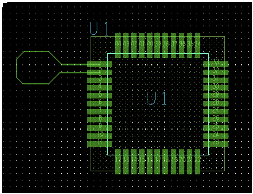
- Netlist the captured circuit and route the only natrest in PCB Editor ()
- In your report explain the procedure to create schematic symbol, package footprint with corresponding figure, the netlisting result, and the circuit PCB layout like . In all these figures
QFP_<your-initials>should appear instead of U.
Question 3: Create a Multi-Layer Board for the Supplied Schematic Circuit
The circuit shown in is designed to amplify an input analogue signal and convert it to digital by the microcontroller for subsequent digital signal processing.
- Draw the schematic circuit in using Capture CIS
- Name the project with your initials so that in the next step the PCB layout file appears as
<your-initials>.brd
- Name the project with your initials so that in the next step the PCB layout file appears as
- Use the schematic symbol designed in Question 1 for Op-Amp as well as schematic symbol/footprint designed in Question 2 for the microcontroller. For the rest of components use the footprints in Table 1
- Netlist the circuit
- In PCB Editor define a 6-layer stack-up that consists of:
- Three power supply planes including VPOS and VNEG for Op-Amp and VDD for microcontroller
- One GND plane
- Top and Bottom signal layers (They appear in the default stack-up)
- Do not forget screen shot of your stack-up for the report!
- Change the colour of plane layers to light colours, (Take screen shots for your report)
- Place the microcontroller, Op-Amp, and the two connectors only on a maximum 2”×3” board
- Place connectors close to the edge of the board so that in 3D image you can see the cross connections to plane layers
- Route the natrests
- Make sure your initials will be etched on the copper (top layer) on the board
- This will differentiate your board from other boards
- Take a screen shot image of your PCB layout for the report
- Generate a side-view 3D image of the board so that the connections of 5-pin connector to inner planes are visible (record the screen shot for your report)
- Note: 3D sideview is not available in OrCAD 17.4. Please use a drawing tool such as Paint 3D or Powerpoint etc to draw the sideview of your multilayer board
- Submit
<your-initials>.brdfile on Moodle - Generate Gerber files and submit in Moodle
- In your report explain how you apply Engineers Change Order (ECO) if requested after finalising the PCB layout (use lecture notes and the unit reference book to find further information)
- Generate Bill of Material (BOM) for this circuit and record it in your report. (use lecture notes and the unit reference book to find further information)
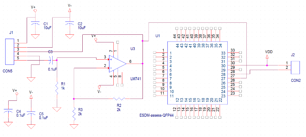
Table 5: Schematic Symbols and Footprints
| Component | C1,2 | C3,4,5 | R1,2,3 | U3 | CON2, CON5 |
|---|---|---|---|---|---|
| PCB footprint | ck17-10pf | smdcap | smdres | soic8 | Jumper2, Jumper5 |