Design/Submit Layout
Create and Edit Footprint.
Introduction
In order to netlist a circuit and design its PCB layout from the schematic circuit diagram, at least two types of library files are required. You learned how to create/edit the schematic symbol library files in the last lab session. You will learn how to create/edit footprint library files in this lab session.
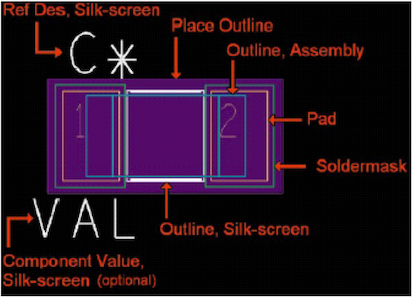
The first step is to create padstacks (.pad file) using Padstack Editor based on the specifications provided in datasheets. Next you will practice how to place pads in appropriate geometries using PCB Editor to create footprint libraries (.dra and .psm files) for discrete components and IC packages.
1. Design a Padstack for Through-Hole Pins
shows a datasheet snapshot of a carbon resistor that was introduced in lectures as one of the very basic electrical components. The final aim of this section is to design a PCB footprint for the resistor. Hence, we need to first create a through-hole padstack that fits the resistor leads. The diameter of component leads determines the drill diameter that is needed to make a hole. The number of layers and electrical connectivity of this component to the layers can also be defined in padstack editor.
- Run Padstack Editor () from start menu → Cadence Release 17.2 → Product Utilities → PCB editor Utilities.
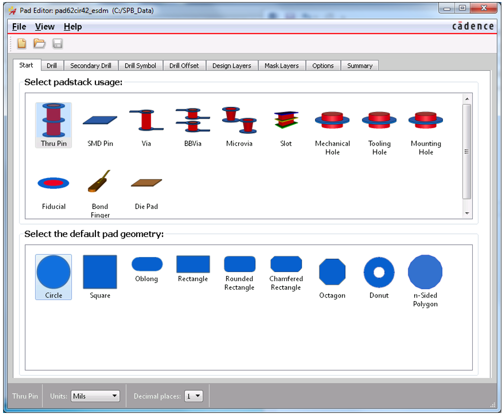
In the first tab, several pad types are listed. The most commonly used pad types are for creating through-holes and surface mount device pins.
- Select Thru Pin and for the pad geometry select circle.
- Select Mils for the units. (It depends on which unit is more convenient for you based on the information provided by datasheet. In this case the resistor datasheet is based on mils)
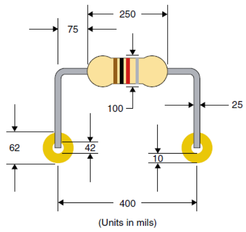
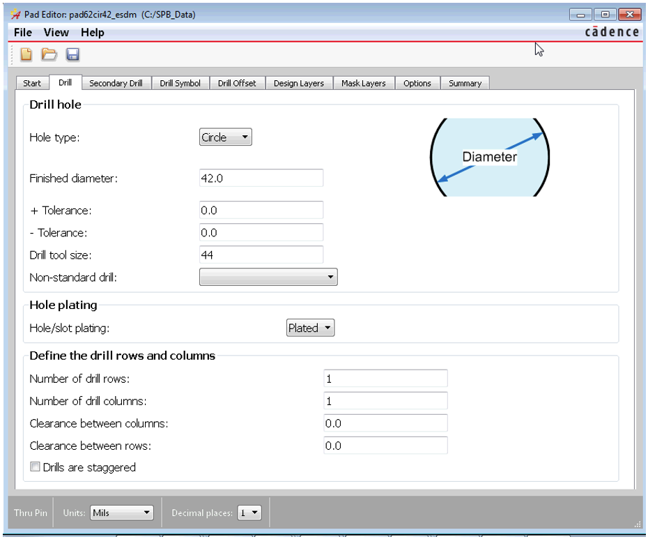
- Click on Drill menu to set up the size and shape of drill hole as shown in . Fill in the empty spaces with the provided attributes. Setting the finished diameter to 42mil and the drill tool size to 44mil allows extra 2mils for the thickness of plating material. As described in the lecture slides, there are four combinations for the padstacks with regard to pad and plated drill that have different applications. In this padstack the drill hole will be metal plated and it will have solder pads at the top and bottom.
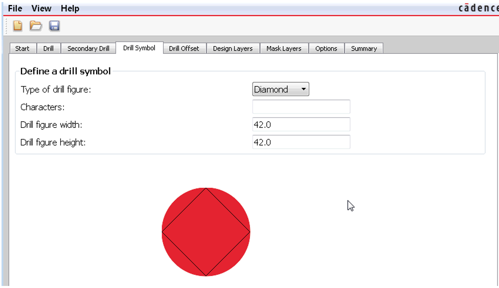
- Select the drill symbol menu and select diamond and set its width and height to 42 (equal to the hole diameter) as shown in . The size of the drill symbol is not critical but is typically about the size of the drill diameter or a little smaller. Note that the drill symbol will not be visible when you ultimately place the component on the board.
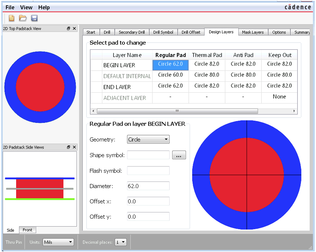
- Switch to Design layers tab (). Here the electrical/thermal connections of a pad to the board layers are defined. In this tab, the shape and size of pads are determined individually. Adding further layers is made possible by right click on each layer and selecting insert layer below/above. In this example the two default layers are enough to describe the pad structure. On the left side of padstack editor, a top and side view of the pad are illustrated that helps in understanding the pad structure.
-
Fill in the pad attributes by left clicking on each pad and selecting its shape from the drop-down menu and setting its size in accordance with . The following explanations addresses some general rules about the size of pads. In order to keep it simple just set the value of thermal, anti and keep out pads 20mil larger than regular pad that solder the component lead to the board.
- Regular pads. The values on the internal layers can be identical to the outer layers but often they are slightly smaller (anywhere from 0 to 20 mils difference in diameter depending on the size).
- Thermal reliefs. The native padstacks in the symbols library typically use circles that are the same size as the antipad. Circles work for positive planes but not for negative planes. For negative planes you need to use Flash symbols. Flash symbols are described later, so for the time being leave the thermal relief as a circle. The procedure for defining padstacks that have no thermal reliefs (i.e., completely connected to a plane) is described later.
- Antipads. The clearance between a pad (or hole) and the surrounding copper (e.g., on a plane layer) should be similar to or larger than the trace spacing constraints you will likely use in your design. A typical clearance diameter is 10 to 20 mils larger than the pad diameter. Note that, if you make an inner pad much smaller than the outer layer pads, the antipad on the inner layer should still be larger than the largest pad in the pad¬stack; otherwise undesirable capacitive coupling can occur between the larger pad and an adjacent plane layer.
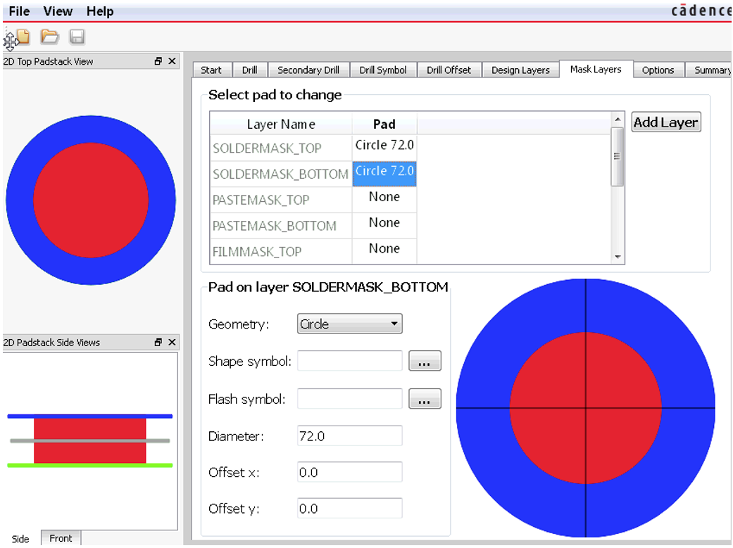
Mask layers can be defined in the next tab as shown in . The difference between solder mask and paste mask is explained in lecture 2, 3.
-
Soldermasks. Soldermask openings are usually a little larger than the outer pads so that registration tolerance errors will not cover any of the pad. The exact amount really depends on the capabilities of your board manufacturer, but in general the soldermask opening is typically 10 to 20 mils larger than the outer pads.
- Set the values of solder mask diameter to 72mil. The component is through hole, hence, there is no need for the paste mask in the padstack,
- Save your work as a .pad file to the PCB Editor symbols folder or your working folder under the following convention:
pad62cir42-<initials>(where initials is your Bath University username) C:\Cadence\SPB_17.2\share\pcb\pcb_lib\symbols
At this stage the design of padstack is finished and we only need to use it for designing a footprint in the next step.
2. Design of Footprint for Through-Hole Components
Design of footprints include defining the position of each pad with regard to other pads as well as the position of the whole footprint on the page. It starts with placing the designed pad in a blank page in PCB-Editor.
- Open PCB Editor Lite,
- From the File menu select New,
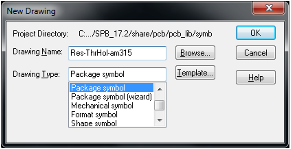
- A new window appears as shown in , where you can supply a name for the component such as
Res-Thrhol-<initials>and choose package symbol as the drawing type.
The drawing area should fit the dimensions of target components. In order to setup this area:
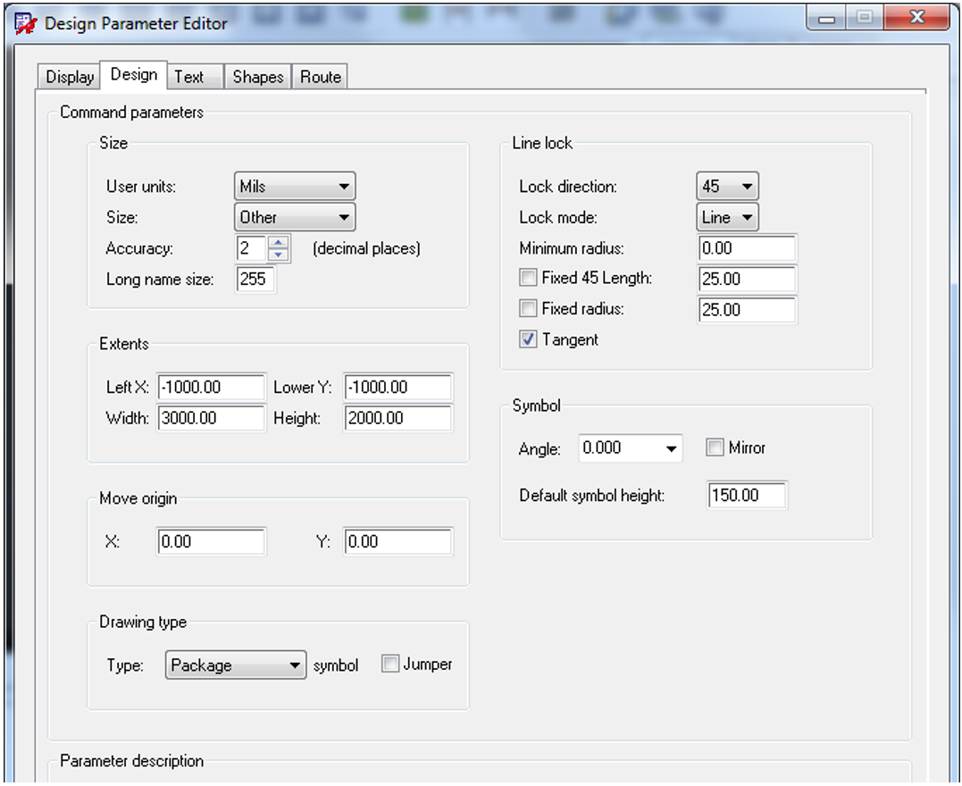
- From Setup menu select Design Parameters and switch to Design tab as shown in .
- Fill in the required parameters in accordance with the values in and click apply
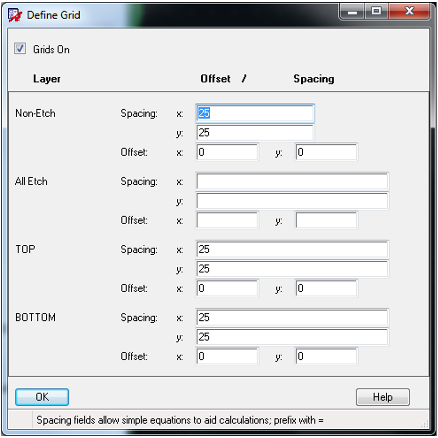
- Switch back to Display tab on the same window and activate the grid (tick Grids on) if it is not already activated. Click on Setup grids and make sure all spacings including etch and non-etch are 25 mils in x and y direction as shown in .
- Now press Ok, and Ok
- To confirm the area settings, move the cursor to the extents of the page and check “current mouse coordinates” at the bottom of your PCB Editor window (from -1000mil in the left to 2000mil in the right). This ensures that the coordinates centre is somewhere at the middle of your design area.
The design area is now ready to place the pads. The next step is to find and place the appropriate pad that was designed in section 3-1.
- To ensure that the created padstack file (.pad) in section 3.1 is saved in the appropriate folder, use your windows explorer to find it in the following folder:
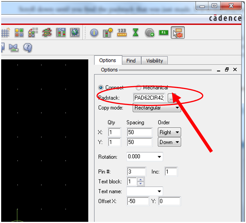
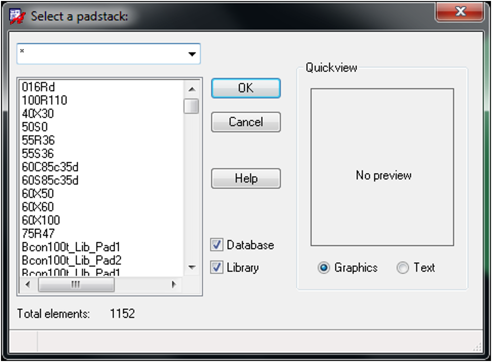
C:\Cadence\SPB_17.2\share\pcb\pcb_lib\symbols. If you couldn’t find it in this folder you will need to find it wherever saved by Padstack Editor and copy the .pad file in this folder. If your computer did not allow you to save the pad file in C drive, try to use a similar pad from the native library. However, submit the pad file that you created in Moodle. - In PCB Editor, select Layout from the menu and select Pins. It changes the Options pane at the right side of PCB Editor as appeared in . Left click on the radio button shown by an arrow in to open a new window for selecting required padstack.
- This window points at Symbols folder, where you should save your padstack by Padstack Editor.
- Scroll down on the window shown in , until you find the padstack that was just created in section 3.1. If it is not displayed, make sure the Database box is checked.
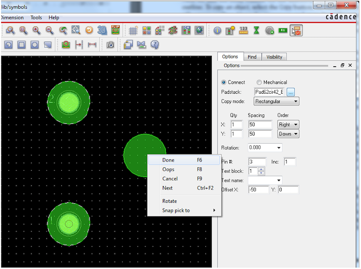
- Click Ok if you find the correct padstack. A padstack will be attached to your mouse pointer. Place the first padstack by clicking and releasing your left mouse button at location (0, 0). Another padstack will be attached to your mouse pointer. Place the second padstack at location (400, 0) then right click and select Done from the pop-up menu as shown in .
The next essential step is to define the outline of the component (resistor).
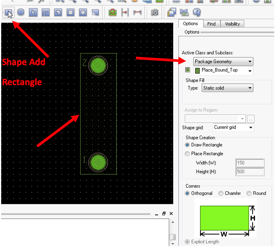
- From Options pane on the right side of the PCB-Editor window, select Package geometry on the drop down menu as shown in .
- Select Place_Bound_Top from the next drop down menu.
- Select Shape Add Rectangle from the tool bar.
- Draw a rectangular around the pads as shown in .
If you save the footprint at this stage, software generates an error message that shows the Reference Designator is missing. This is the third essential element in defining a package footprint that relates the footprint symbol to a corresponding schematic symbol.
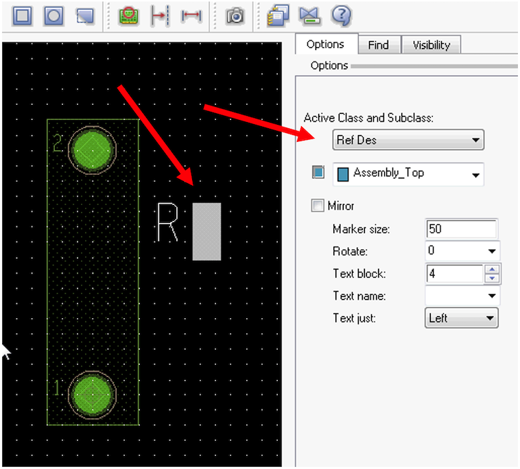
- From Layout menu select Labels and then RefDes
- Option pane changes to RefDes as shown in , while the cursor is a text tool now. Click on a side of the device footprint and use keyboard to input the reference designator, which is typically R. In this case you type in
R_<your initials>. Right click on the layout and select Done in the pop up menu. - Save the footprint.
Required steps to create a footprint are achieved now and you can save the footprint. However, the current situation of the designed footprint may cause some practical limitations in manufacturing processes. For example without the package outline data on the board silk screen, it is hard to appropriately place IC packages or components with a certain polarity during assembly.
To draw silk screen outline of the package on top layer:
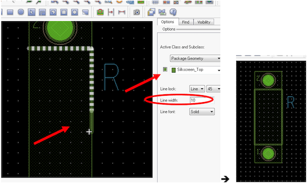
- select the Add Line tool ()
- select the Package Geometry class and Silkscreen_Top subclass from Options pane, and select a Line width of 10 mils, as shown in .
- Note: if you keep 0mil as the line width, there will be no visible rectangle in the generated artworks later on.
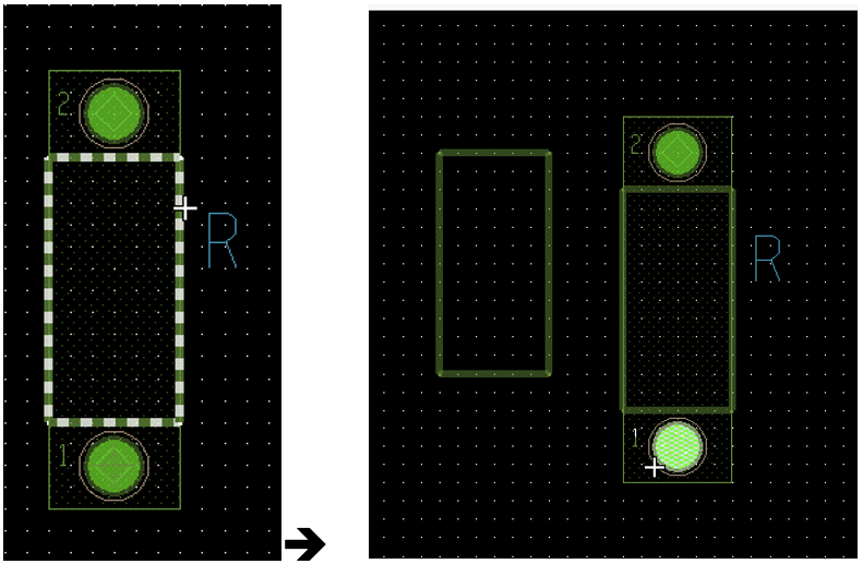
It is possible to add different layers with similar size on top of each other. It is recommended to use different colours for recognition by designer. For example:
- Select copy from tool bar, hover the mouse cursor on the silk screen top rectangle that you created in the previous step. Select it by a left click when it is highlighted and click on the highlighted rectangle. Move your mouse cursor around. It holds to a new rectangle that can be placed wherever you left click.
- Place the copied rectangle somewhere with minimum overlap with other components as shown in . Right click and select Done from pop up list. This ends the copying mode.
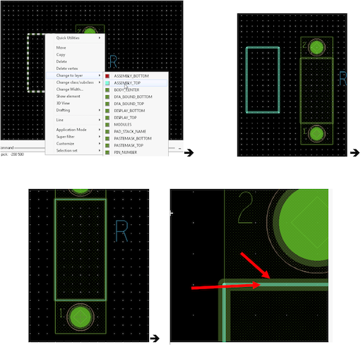
- Select the copied rectangle by dragging mouse around it while the left button is pressed. Right click on the highlighted (copied) rectangle. Select Change to layer and then select Assembly Top, which is in a different colour as shown in .
- Select the rectangle again to change the width of rectangle (Select the rectangle, right click and select change width from pop up menu). A new window appears in which you could change the width of rectangle from 10mil to 3mil.
- Right click on the “assembly top” rectangle and select move from the pop up menu.
- Left click to place the assembly top rectangle on silk screen rectangle as shown in .
On a magnified image in , the two overlapping layers are shown by two arrows.
- Save the footprint,
- Submit the created files (.pad, .dra and .psm) in the Moodle page.
Extra Exercise
3. Editing a Native Footprint Library
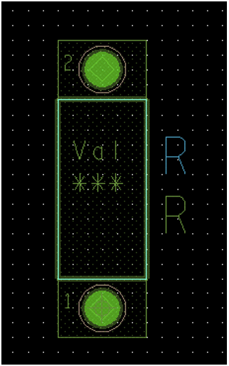
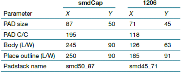
The native PCB Editor library (symbols folder) contains limited surface-mount footprint symbols for resistors and capacitors. These capacitor and resistor footprints are roughly the 2010 and 1805 sizes, respectively. However there are many other resistor/capacitors in the market that might suit better for your potential applications. We could start from scratch and create our own library database; but since they have many similar features, we start with an existing native library file and just modify it. In this section, we start with an existing smdcap footprint and modify it to make a size 1206 footprint.
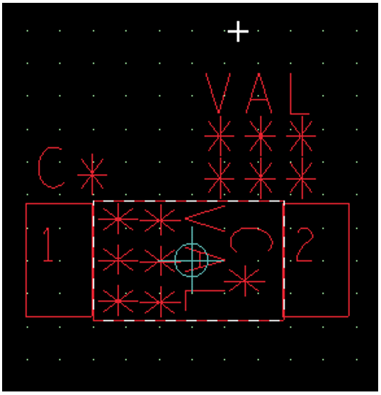
- Start PCB Editor and open smdcap.dra located in the symbols library. compares the smdcap symbol with the requirements of a 1206 chip capacitor. The closest equivalent padstack as defined in for a size 1206 capacitor is smd44rec72. We use that as a starting point for a smd45rec71 padstack.
- Start Padstack Editor, open smd44rec72 and Save it as smd45rec71 in the symbols library.
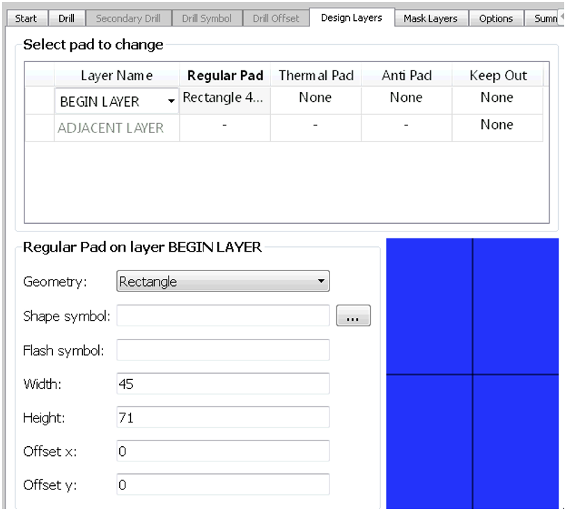
- Select the Design Layers tab and change Begin layer (top) dimensions as shown in . Save your changes (File → Save from menu).
- Select the Mask layers tab and change the width and height of Solder Mask top to 55mil and 91mil, respectively. Save the modified padstack.
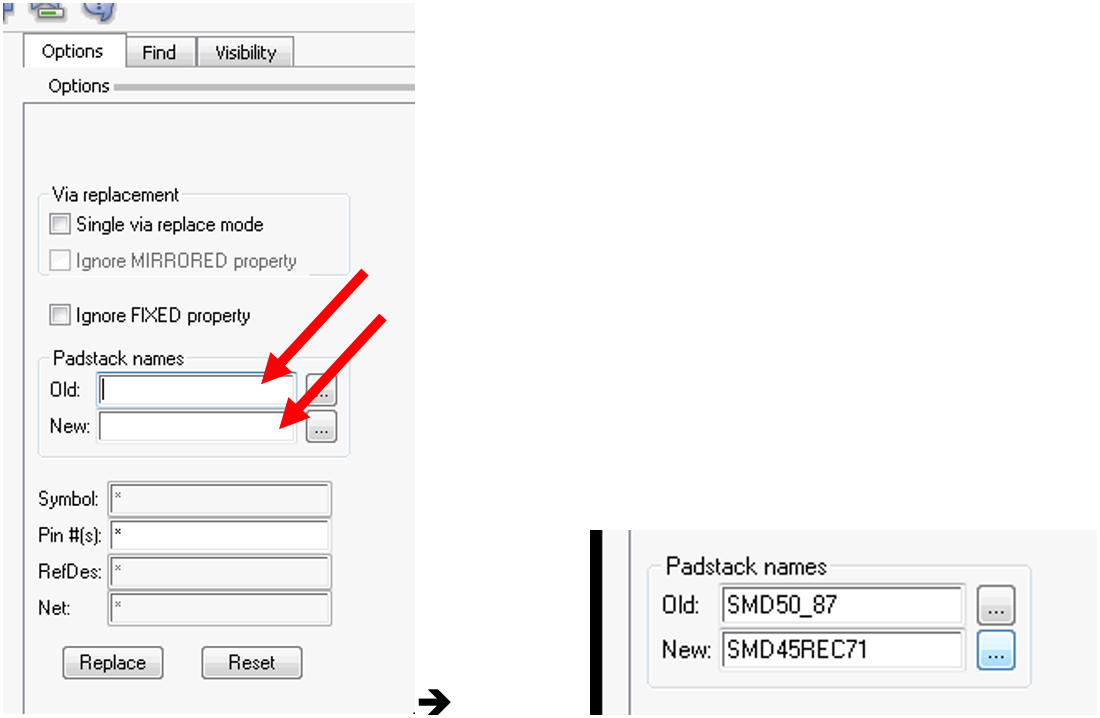
- In PCB Editor (while smdcap.dra is open), from Tools menu, select padstack and Replace. Options pane changes to (left).
By left click on any pad you can supply its name in the Old field and by clicking on the radio button in front of New field you can choose any padstack available in the library.
- Select either pad 1 or 2. This fills smd50_87 in the Old field. Then enter the pad you just designed, and saved in symbols folder, in the New field. These fields should eventually look like (right).
- Click on Replace. At this stage you should notice the difference on pad size.
- Save the footprint as
smdcap-<your initials>. - Submit the corresponding .dra and .psm files in Moodle.