Footprint Libraries in OrCAD
Netlisting Circuit Schematic and Layout Design in OrCAD.
Introduction
In the following example, you will;
- Become further acquainted with digital libraries for component schematic symbols and PCB footprints and the necessity of library development.
- Learn some guidelines about placing the components with regard to Design for Manufacturing
The prerequisite of this lab is OrCAD Design Flow in the previous sessions.
Design Example
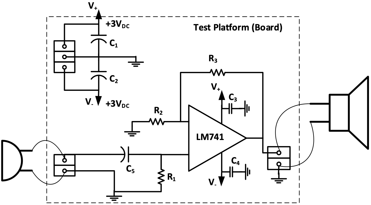
A new microphone, which is designed by the research and development (R&D) sector of a start-up company, needs a test platform for performance evaluation. Microphone is an electromechanical transducer that converts the mechanical vibrations in the air to a small electrical signal. The test platform must increase the signal amplitude to be large enough for further processing and/or applying to a speaker. Therefore, the platform consists of an audio pre-amplifier, a power amplifier and a speaker. In this unit we will target the PCB design skills rather than the details of electronic circuit design, which is beyond the scope of this unit. Hence, let’s ignore the power amplifier and assume that pre-amplifier will drive the speaker directly. The electronic circuit diagram for this platform is shown in (), which demonstrates an analogue amplifier circuit.
The PCB designer must ensure that the effects of external noise sources and interferences, which degrade the desired signal quality, are minimised by applying certain design techniques. However, the focus of this design is on the Design for Manufacturing requirements (see page 77 of reference book for further explanations1). Design for Signal Integrity will be discussed in Electronic System Design and Manufacture 2.
1 Complete PCB Design Using OrCAD Capture and PCB Editor, By Craig Mitzner
This ebook is available online at http://www.bath.ac.uk/library/
Instructions
- From Start Menu in Windows find Cadence Release 17 → OrCAD Lite Products and run Capture CIS Lite.
In order to create a new project:
- From File menu → New → Project
- Select Analog/Mixed Signal → Create a blank project and name it as
ESDM1_lab6_<initials>.- From now on wherever in the manual you see
<initials>replace it with your Bath University username. - Note that this exercise is not intended as PSpice simulation. For example, PC Board Wizard could be used instead of Analog/Mixed Signal for this task.
- From now on wherever in the manual you see
- If it didn’t automatically open the schematic window, from project manager tree click on design file (.dsn) → SCHEMATIC → double click PAGE1
-
Make sure Grid is activated from View menu.
- In order to draw the following schematic circuit () in Capture you will need to: 1) find components in the library, 2) place the component on the page and 3) connect the component pins by wire to each other. The circuit in is modified to ensure that all component footprints are available in standard OrCAD library
- From Place menu select Part,
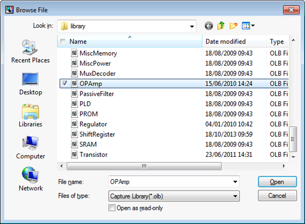
- In order to access the component schematic symbols, the corresponding libraries should be added first. Use the library adder icon (shown in ) (Ctrl+A) to access the appropriate libraries. For example the amplifier can be found in OpAmp library. Therefore after reaching the window in , browse for the OpAmp in this address:
C:\Cadence\SPB_17.2\tools\capture\library

- Choose LP111 from the Part List and double click to place it on the schematic page.
- Repeat the same procedure for the other components
- Similarly choose the headers CON5 and CON2 from Connector library as well as resistors and capacitors from Discrete library.
- Choose the correct ground and power supply symbols from the selectable icons on the right side of Capture window (), or find them from the Place menu.
- Use the wire tool to connect the components as shown in Figure 3.

- Save the schematic.
- In order to netlist the circuit and prepare it for the layout phase, the schematic symbol of each component should be assigned by a corresponding PCB footprint that exists in the PCB footprint library, which is usually located in
C:\Cadence\SPB_17.2\share\pcb\pcb_lib\symbols- Double click on each component schematic symbol; It opens a new table
- In the PCB footprint box, enter the corresponding footprint from
- Table 1 for each component
- Save the design
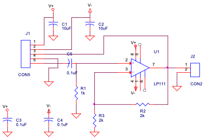
Table 1: Schematic Symbols and Footprints
| Component | C1,2 | C3,4,5 | R1,2,3 | LP111 | CON2, CON5 |
|---|---|---|---|---|---|
| PCB footprint | ck17-10pf | smdcap | smdres | soic8 | Jumper2, Jumper5 |
- Switch to the project manager window and click on PAGE1 to highlight it. From Tools menu,
- Annotate,
- Design Rule Check and
- Netlist the board.
Reminder: in the last step make sure Create PCB Editor Netlist, Create or Update PCB Editor Board (Netrev) and Open Board in OrCAD PCB Editor are all activated (ticked) as shown in .
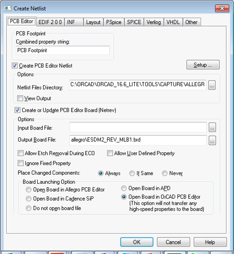
This will automatically open up the PCB Editor Lite.
- From the Setup menu select grids and make sure the grid is on and 100mil (2.54mm) is applied for non-etch spacing, click Ok,
- Select the rectangular drawing tool,
- On the options pane at the right side of the PCB Editor window select Board Geometry → Outline,
- Draw a 50mm x 40mm (1968mil x 1575mil) outline for the board.
- Place all your components in the defined outline,
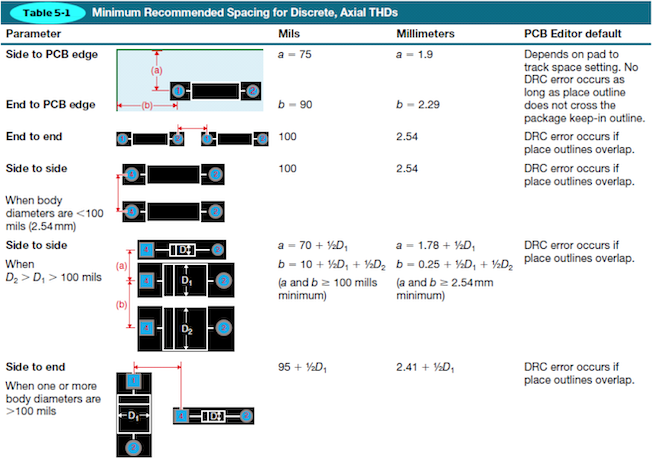
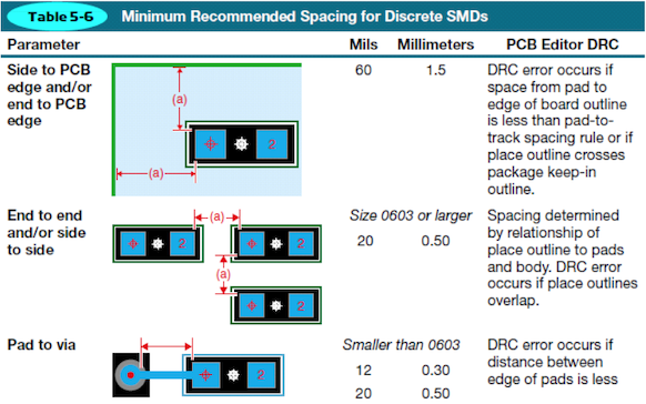
- Try to use as much information as you could from and to ensure that placing the components is in accordance with manufacturing regulations. For example capacitors C1 and C2 are THD (see ) while other resistors, capacitors and the OpAmp are SMD components (see ). Further explanations are available in your text book.
- From Route menu choose Connect tool to connect the components on the Etch layer.
- Try to avoid right angles in connections.
Go back to the Capture environment and change the amplifier with LM741 from OpAmp library and supply the “correct” PCB footprint (soic8).
- Make sure the PCB Editor window is closed,
- Netlist your circuit,
- Think about how to mitigate the error/warning generated by Natrev.
This will be discussed in the following lecture.
Create and Edit Schematic Symbols
1. Modifying Schematic Symbols
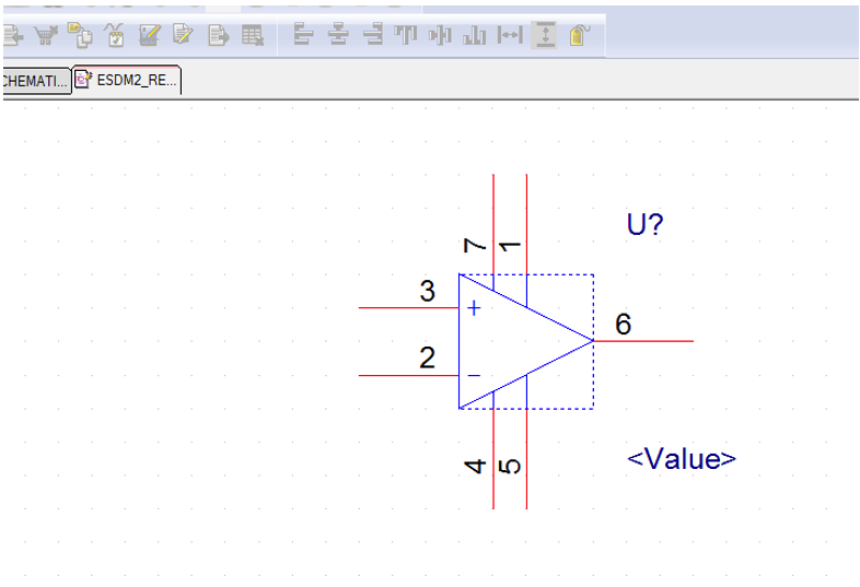
From a circuit design point of view, LM741 is the appropriate package to use in the test platform you designed last session. However, from a manufacturing perspective, to avoid the DRC error below any 8-pin surface mount (SMD) package with an identical footprint could be replaced by a LM741.
DRC error:
#1 WARNING(SPMHNI-192): Device/Symbol check warning detected. [help]
ERROR(SPMHNI-196): Symbol 'SOIC8' for device 'LM741_SOIC8_LM741' has extra pin '8'.
This software error means that the footprint has 8 pads while the schematic symbol has 7 pins. You could check this by opening the soic8.dra file individually in PCB editor. Hence we replaced it with LP111 in the previous lab experiment.
What if we could not find any schematic that represent the Op Amp footprint correctly?
Now we aim at taking a more versatile approach to fix the inconsistency that exists between the schematic and footprint of LM741. After you learn how to do this, modifying or creating any other inconsistencies will be straightforward.
- Open the schematic file of the previous lab session. If you have not saved your design, redraw the schematic diagram in with LM741 as the amplifier component.
- Check that if the OpAmp footprint is soic8.
- In order to edit the schematic symbol, click on the part schematic to activate it, then right-click and choose Edit Part as shown in .
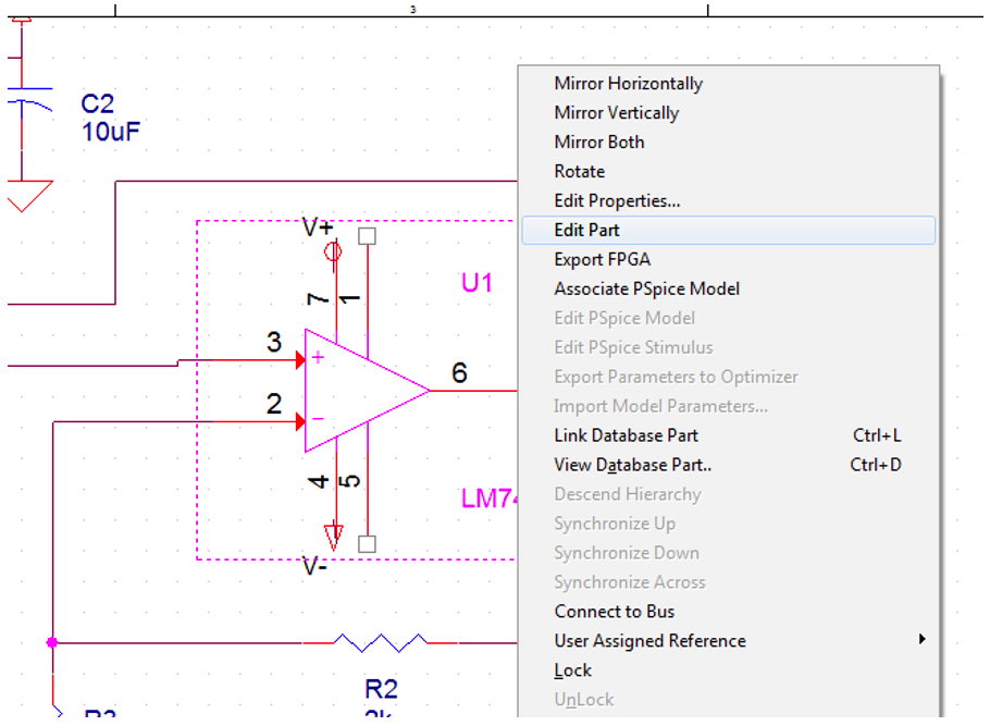
This opens the selected schematic symbol in a new window as shown in , where you can modify the part appearance and its pin configuration. For example, users can move around the pins of schematic symbols by simply clicking and dragging the pin, which is impossible anywhere else in Capture environment in particular in the schematic circuit diagram pages.
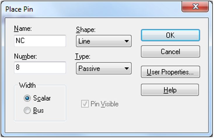
The pin name can be extracted from the datasheet that is NC (not connected) in this case. This name should be expressive but you can use any other alphanumeric characters. Though the pin number should be compatible with the pad number of the corresponding footprint. For the pin shape Line is recommended as it looks similar to other pins and for the pin type, any selection makes no difference (why?). After clicking on OK, a pin will appear on the cursor. Click at the edge of the Op Amp schematic to connect the pin to the symbol as shown in .
- Right click at some blank part of this window and select End mode (this could be done by pressing Esc as well).
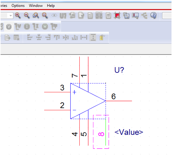
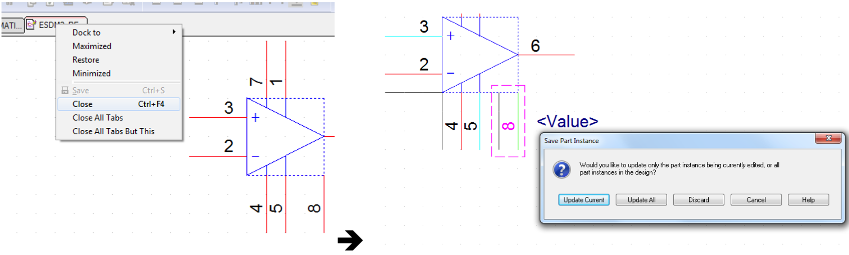
While closing this new tab, OrCAD will ask you to update the schematic symbol.
- Choose Update current and this will save the changes to the component in this schematic as shown in .
- Now annotate and netlist the circuit and check if it is error-free.
- Make sure the PCB-editor window is not open at this time.
2. Creating Schematic Symbols for Components
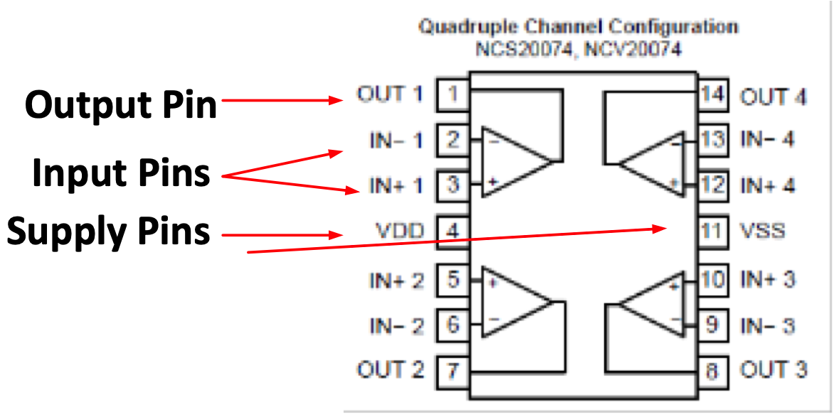
One of the most important achievements of integrated circuit (IC) technology is the capability of implementing several identical components (of one type such as transistors) on a single chip with minimal mismatches in their characteristics. Therefore it is very common to have IC packages that contain many identical components. In these circumstances for the component schematic, it is possible to make the schematic symbol for only one part and let the software repeat it whenever required. In this section we will draw a schematic symbol for a Quad Amplifier IC package. It consists of four OpAmp parts that each has two inputs and one output pin. The whole package has two power supply pins as shown in . The complete datasheet is uploaded in Moodle.
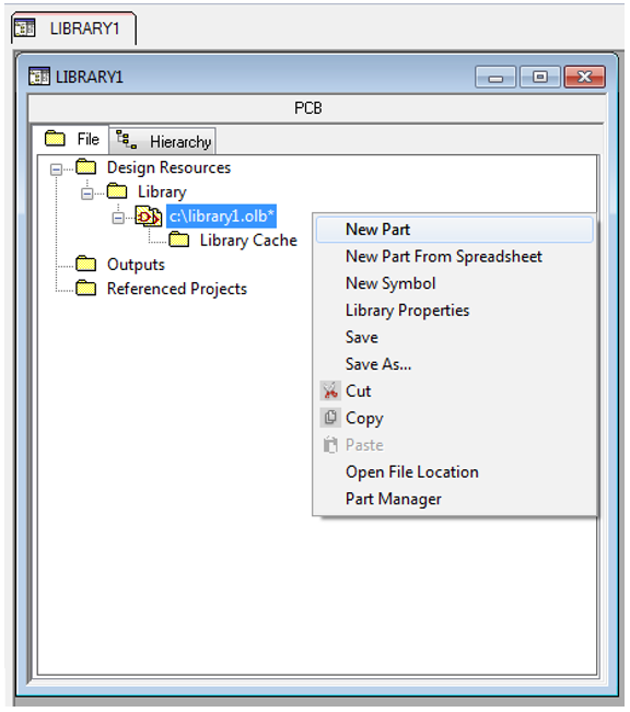
- From File menu select new → Library
- In the project manager window a new library file (.olb) with default name “library1” will appear as shown in .
Based on the material in lecture 2, this is the first method of creating a schematic representation for any component.
- Right click on the file name and choose new part. It will open a new window that represents the basic properties of the new component ().
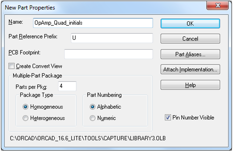
- Add the component name. This name should describe the component. Here include your own initials or Bath University username in the component name (example:
Quad-Op Amp-AM3151). - The part reference will appear as reference designator with a number suffix that indicates the number of parts of this type. U is commonly used for IC packages.
- The package consists of four identical Op-Amp parts; so select Homogeneous and fill in 4 for the number of parts in this package.
Clicking on OK should open a new window where you have access to drawing tools such as straight line, arc, rectangle etc. on the right side of the window. These icons are also accessible from Place menu as well.
- Make sure snap to grid is de-activated from the toolbar at the top of the window. It will make the curser flexible while drawing graphics.
- As mentioned in lecture 2, the graphics of only one component needs to be created here and the software will make the other three. Choose straight line tool from the icons in .
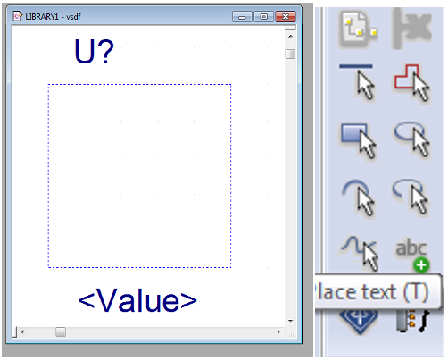
- Draw a triangle as shown in .
- Next use the Pin tool from Place menu to add the pins with regard to the pin configuration in above. Here we only create the first Op Amp, which requires five pins including 2 inputs, 1 output and 2 power supplies. Therefore, while adding the pins you should match the pin numbers and types with the datasheet configuration.
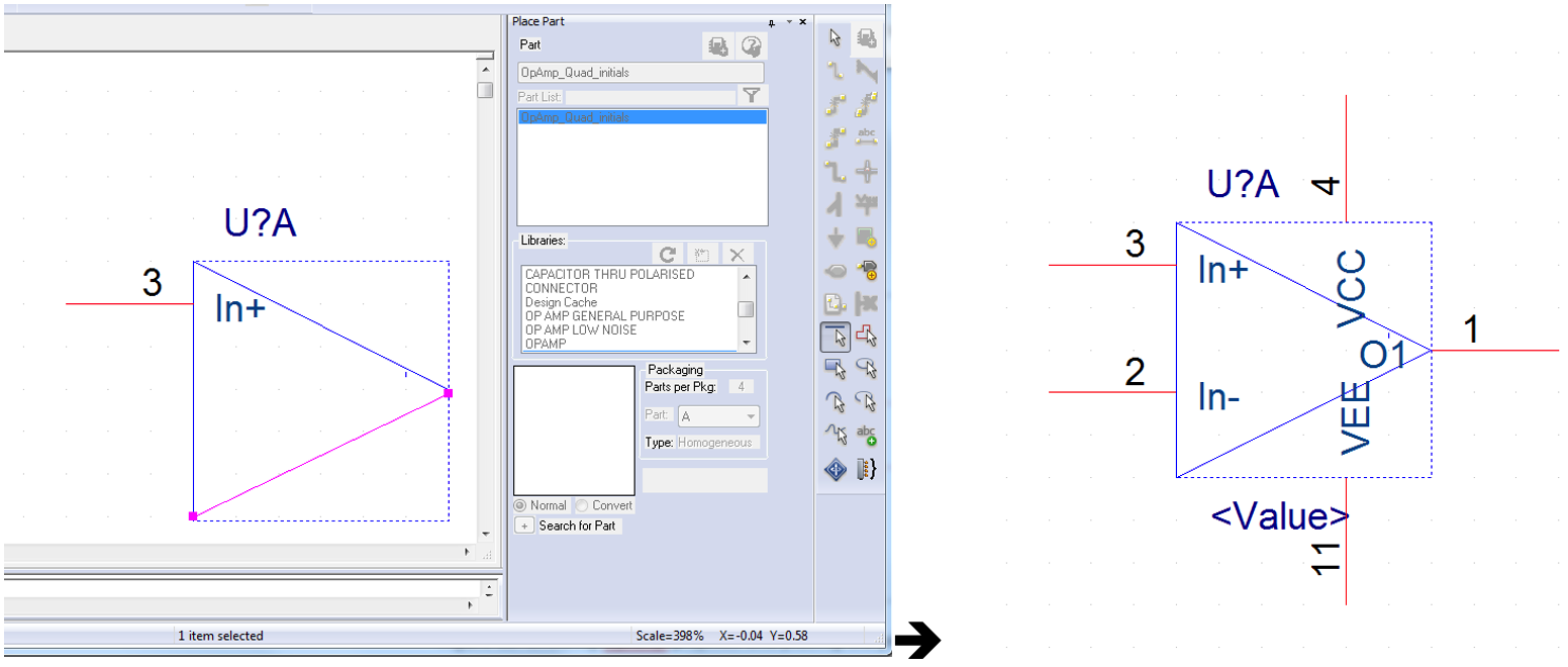
- After finalising with a schematic like the one on right hand side of , close the tab and save it ( above).
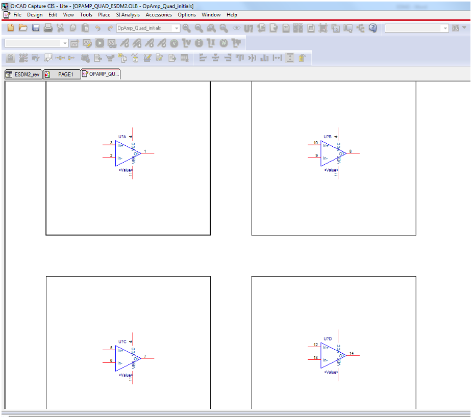
- Open the library file from project manager window.
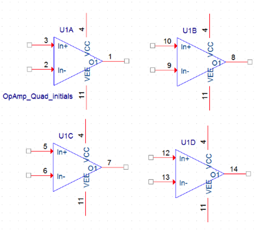
- From the View menu select the package view that shows all four parts in one window as shown in . Double click on each part you choose and edit its properties, importantly each Pin name and its number.
- In order to test the validity of the schematic library, use it in a schematic circuit.
- Create a new project
- Draw a sample circuit schematic. This consists of only the new component (
Quad_OpAmp_<Initial>). - Now fetch this component from the library () in a new schematic circuit diagram.
- After selecting one of the amplifiers in the library by double left-clicking, the cursor turns into OpAmp schematic. With the cursor over the desired position of the amplifier, left-click to make the Op Amp appear, as shown in .
- Assign an appropriate PCB footprint to the schematic component such as soic14.
- Save your design, annotate and netlist it.
- Check whether it is possible to place the appropriate footprint in PCB Editor environment. We don’t expect any warnings/errors!
- Submit the schematic file, which has your initial in the file name, in Moodle.
3.
A second approach to design schematic symbols of electrical/electronic components is to use a spreadsheet and fill in the pin properties directly from datasheets. This method is highly popular when there is a large number of pins and it is also possible to copy the pin numbers and descriptions directly in the spreadsheet. Example application is digital ICs such as memory units (RAM: Random Access Memory) or microprocessors.
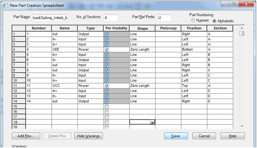
Let’s repeat the previous exercise by using a spreadsheet to create the quad amplifier schematic. From the project manager window right click on library and select New part from spreadsheet (). A blank spreadsheet will appear. This method is by default designed for heterogeneous component, however, it could be used for homogenous components as well.
Name the component as Quad_OpAmp_initials_b (b is to differentiate it with the previous package designed in graphical mode). No. of Sections determine the number of parts in a package (4 in this case). Fill in the pin numbers, names and other properties as shown in the datasheet. The power supply pins could be repeated for each part in the package. However, OrCAD Lite version is limited by maximum 14 pins in this approach.
Click on save after filling in all required attributes. Double click on the new component library in project manager.
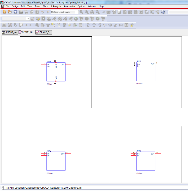
The result should look like after choosing the Package view. It is possible to open each section in a graphical editing pane and change the rectangular appearance of the parts to triangular.
- Submit your library file in Moodle page.
4.
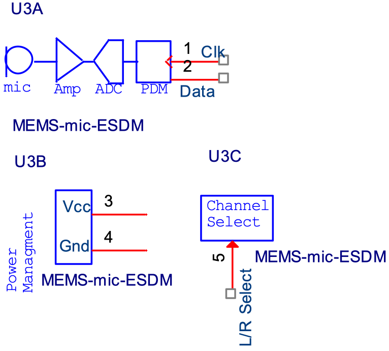
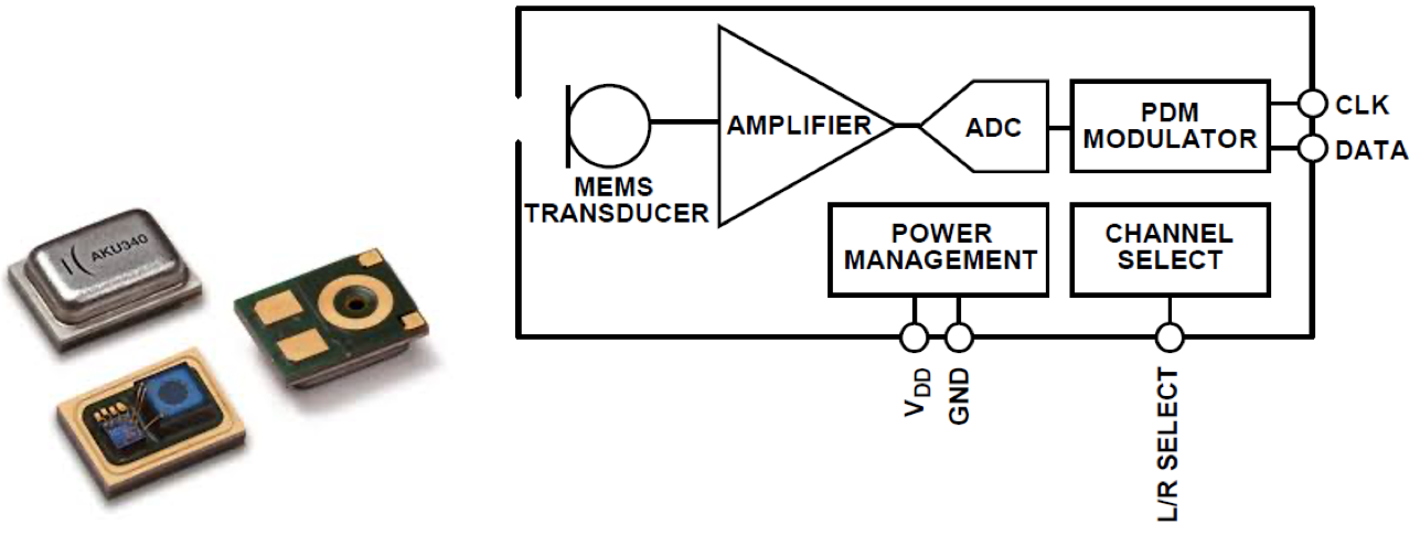
A high specification digital MEMS (Microelectromechanical Systems) microphone that is designed and made by a research group doesn’t have any component schematic/footprint in CAD libraries (). The design of PCB for such a high sensitivity mic is of great importance to make it immune against interference.
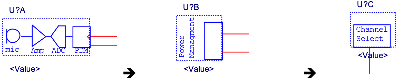
It is recommended to draw this component as a heterogeneous package since each part might appear on a different circuit schematic diagram while it represents one single component as shown in . Using graphical method, draw the following schematic in a three part heterogeneous package. After selecting new component a graphical environment () but with label U?A will appear. After designing this part use next part from view menu to proceed to the next parts so U?B and U?C.
- Add the component to the library
- Place it on a schematic diagram
- Submit the schematic library in Moodle.