Characteristics of Operational Amplifiers in Simple Linear Feedback Circuits
Introduction
The aim of this experiment is to help students gain familiarity with the use and application of operational amplifiers in simple linear feedback circuits of practical importance. This experiment focuses on the characterisation of non-linear features of the amplifier, where the output is distorted. The distortion limitations of an amplifier, or many electronic devices, can be a significant limitation to their use. The experiment, which should be recorded in real time, assumes a basic theoretical knowledge to the level taught in the EE22004 course. The lecture notes for this course are available on Moodle.
List of Experiments and Recording
In this experiment you will be examining the Inverting amplifier and looking at:
-
Saturation and clipping effects.
-
Slew Rate effects.
-
Input offset effects.
There should be sufficient time in the three hour laboratory sessions for all measurements to be taken, recorded graphically where needed, and discussion of the results developed. You need to keep a log of your experiment capturing all of your results, analysis and discussion, with sufficient detail to allow repetition of your experiment.
Please note that while it is basic laboratory technique to record as much data as possible in real time, many students choose to complete their graphs and complement their discussion and conclusions in their log after the event, and this is perfectly acceptable. A formal written report is not required, but your log is the basis of the information needed to provide evidence of attaining various levels of skills in Mahara.
Preparation before beginning the experiments
You should be familiar with the first experiment on the linear features of amplifiers. You should have access to, and be familiar with, the following standard laboratory instruments:
-
DC power supply
-
Signal generator
-
Digital oscilloscope
-
Digital multimeter (DVM)
-
Box/tray of short wires for interconnecting items
-
Box/tray of components including operational amplifiers, resistors and capacitors.
In addition you will be provided with a prototyping board and you should be familiar with its use and built in connections. Typical supply voltages for the op-amp you will be using (LM-741, TL-081 or equivalent) are ±15 V.
The signal generator provides sinusoidal, rectangular and triangular waveforms at a frequency that is variable (programmable) over several decades. The lower limit of the amplitude range of the generator is 20 mV and its output resistance is $50\,\Omega$. When the signal generator is connected to a $50\,\Omega$ load the voltage applied to the load is half of the source voltage. When connected to an open circuit or very high impedance load the load voltage is the source voltage.
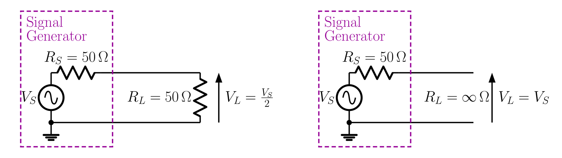
There is a menu setting on the signal generator where you set what type of load impedance is connected to the generator. When set to ‘Low Z’ the signal generator assumes that a low impedance, $50\,\Omega$, is connected and the readout of the voltage is appropriately scaled to $\frac{V_{S}}{2}$. When set to ‘High Z’ the signal generator assumes that a high impedance, open circuit, is connected and the readout of the voltage is appropriately scaled to $V_{S}$. You can check this out by connecting your DVM (which has a high input resistance) directly across the terminals of the generator. In order to allow for this situation, the set-up menu should select ‘High Z’ so the value shown on the generator readout is correct.
The minimum output voltage provided by the generator in ‘Low Z’ mode and terminated in $50\,\Omega$ is 10 mV peak-to-peak (pp) which is rather too high for the experiments where high gain is required. So please connect the generator to your circuit using a divide-by-5 attenuator realised as a potential divider circuit consisting of two resistors. This can be built on your prototype board using preferred resistor values (i.e. one of the normally available values):
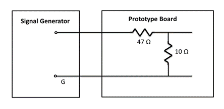
Notice that the input resistance of this divider is 57 Ω rather than $50\,\Omega$ due to the use of preferred values and that the ratio is 10/57 = 0.175 rather than 0.2. These small discrepancies should be taken into account in the interpretation of your results. Remember to set the generator to ‘Low Z’ which will mean that the voltage appearing across its output terminals will correspond with the readout.
Operational Amplifiers - basics
An Op-Amp is a DC-coupled differential voltage amplifier which is generally shown on circuit diagrams as a triangular circuit symbol. The figure below shows the circuit symbol, the simple generic equivalent circuit for an Op-Amp and the outline of the physical packaged Op-Amp when seen from above. The pin numbers used on the packaged Op-Amp are shown on the circuits diagrams as a value in brackets, eg. the output $V_{o}$ is pin 6:
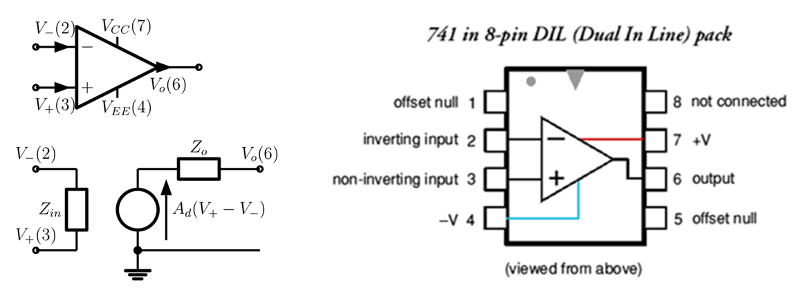
In many circuit diagrams the power supply connections on pins (4) and (7) are omitted. It is assumed that people implementing circuits will know to provide these supplies – otherwise the circuit can not work.
There are many types of Op-Amps and the generic equivalent circuit for the Op-amp is used with different values for $Z_{in}$, $Z_o$ and $A_d$. The Op-Amp has two inputs, the inverting input at pin 2 where the voltage with respect to ground is $V_{-}$ and the non-inverting input at pin 3 where the voltage with respect to ground is $V_{+}$. The output voltage at pin 6 is the product of the differential gain $A_d$ and the difference between the two inputs: $V_{o} = A_{d}\left( V_{+} - \ V_{-} \right)$. For most Op-Amps the currents at the inputs, $i_{-}$ and $i_{+}$, are very small, but finite. With no DC input currents the Op-Amp will not work. Some have an internal bias arrangement so that there is no need for finite DC bias currents to flow into the inputs. The input impedance is often very high, essentially open circuit, while the output impedance is often very low. The differential gain, $A_d$, is often very high and as the output voltage $V_o$ will be a finite voltage between $V_{CC}$ and $V_{EE}$ the difference between the two input voltages is very small, i.e. $\left( V_{+} - \ V_{-} \right) \approx 0$.
The first experiment used the Op-Amp in linear small signal ac amplifier configurations. In other words the dc conditions are chosen as a fundamental baseline and the ac input signal is a small perturbation allowing the amplifier to to be approximated as a linear system. In Op-Amps, particularly at higher output levels, the output is not a faithful replica of the input. As the output waveform is a different shape to the input waveform the circuit is distorting the signal and behaving in a non-linear manner. Non-linear distortion is observed in two ways in this experiment, by looking at the ‘clipping’ of the output waveform and by examining the Slew Rate of the amplifier. Both bandwidth and slew rate place fundamental limitations on the performance of amplifiers but for entirely different reasons.
When a sine wave of frequency $f_1$ is input into the amplifier the output voltage amplitude at $f_1$ is $V_1$. When the waveform is distorted there are also harmonics at the frequencies $n\, f_1$ where $n$ is an integer, with respective voltage amplitudes $V_2,~ V_3, ~V_4, …..$ The Total Harmonic Distortion (THD) is then
\[THD = \frac{\sqrt{V_{2}^{2} + V_{3}^{2} + V_{4}^{2} + \ldots}\ }{V_{1}} = \ \frac{\sqrt{\sum_{n = 2}^{n = \infty}V_{n}^{2}}}{V_{1}}\]Amplifier Experiments
For all the experiments ground is the mid-point of the ±15 V power supplies and all voltage measurements (large signal and small signal) are made with respect to ground. The power supply needs to be used in dual supply configuration.
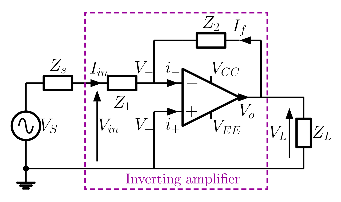
Inverting Amplifier
The circuit schematic for an Op-Amp connected as an inverting amplifier is shown in .
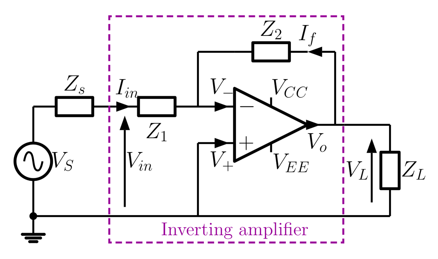
In this experiment the impedances in the circuit will be resistances, so $Z_{1} = R_{1}$ and $Z_{2} = R_{2}$. The closed loop voltage gain $V_L/V_{in}$ of this amplifier is approximately $-\, R_2/R_1$ and it can operate over a wide range of closed loop gains and frequencies.
Note that the DC supplies needed to power the Op-amp are applied at pins (4) and (7), and that the input (AC) is applied at pin (2) or pin (3). When debugging circuits you should always begin by checking the DC levels in the circuit and the continuity of connections between pins (4), (7) (2) and (3) and the relevant outputs on the power supply and the signal generator. You should perhaps check that the supply voltages are measurable on pins (4) and (7) on the Op-Amp and that ground potential (i.e. half way between the power supply levels) is properly defined. Then look at the DC levels on the signal input pins (2) and (3) and the output pin (6). These should all be at ground potential. If all is well, AC signals should be visible on pin (6) but probably not at the inputs as the levels will be too small.
Op-Amp Saturation and Waveform Clipping
To observe this simple form of distortion in an amplifier re-connect the inverting amplifier from the first experiment using a LM-741 operational amplifier but this time choose the two resistors to provide a voltage gain of -10 and an input resistance of $10\,k\Omega$. Use the output from the signal generator without the potential divider and apply 0.5 V (pp) sine wave to the amplifier input at a frequency of 1 kHz. Note and describe the form of the output waveform. Then increase the input signal to 2.0 V (pp) sine wave. Note and describe the form of the output waveform - why is it this shape? This is often referred to as the clipped waveform.
The frequency spectrum of the output waveform can be analysed using the FFT function of the oscilloscope. Using the FFT function on the oscilloscope display the frequency spectrum of the output signal with a center frequency of 9kHz and a span of 18kHz. To produce a well defined signal spectrum there should be many periods of the signal visible across the screen. Reduce the input voltage to 0.2 V (pp) sine wave. Then gradually increase the input voltage to 2 V (pp) sine wave observing the relative size of the 1KHz signal and its harmonics in the output signal. Note how the harmonics vary.
With the input 2 V (pp) sine wave record the relative amplitudes of the fundamental 1kHz frequency and the first 8 odd harmonics. From this determine the THD that the amplifier is producing.
Note on setting oscilloscopes for frequency spectrum measurements
Keysight 1000, 2000 series oscilloscopes: Select FFT. Select channel 1 or 2 as the source depending on the channel you are using. Using the rotating Entry knob set the Span to 18 kHz and the Center to 9 kHz. Set the Window to Rectangular. Set the vertical scale to Decibels. Set the scale to 10dB per division and using the offset set the highest component of the signal spectrum to be at the top of the screen.
Tektronics 2000, 3000 series oscilloscopes: Select Math, then FFT. Set the FFT source to 1 or 2 depending on the channel you are using. Set the Vertical Units to dBV rms. Set the window to Rectangular. Set Horizontal scale using the a and b Multipurpose knobs to give a centre frequency of 9 kHz and a scale of 1.8 kHz/div. Set the Gate to be off.
Slew Rate
For a variety or reasons the output voltage and current have a maximum rate at which they can change with time. This slew rate, $\Lambda_{SR}$, is expressed in units of $V/s$ or $A/s$, and often more conveniently in $V/\mu s$ or $A/\mu s$.
A single frequency sinusoidal signal can be written: $f\left( t \right) = A\cos\left( \text{ωt} \right)$ The rate of change of the signal with respect to time is:
\[\frac{\partial f}{\partial t} = - A\ \omega\sin\left( \omega \,t \right)\]This is steepest when $\sin{\left( \text{ωt} \right) = \pm 1}$ and the gradient or slew rate is $\Lambda_{SR} = A/\omega$. If this gradient exceeds the slew rate of your amplifier the output of the amplifier can not change quickly enough to produce a good copy of the input. The power bandwidth of an amplifier is sometimes expressed in terms of the slew rate, $\Lambda_{SR}$, for the amplifier and the expected voltage amplitude output $A$ as:
\[\omega_{P} = \frac{\Lambda_{SR}}{A}\]Test A
Re-connect the inverting amplifier from the first experiment using a LM-741 operational amplifier but this time choose the two resistors to provide a voltage gain of -10 and an input resistance of $10\,k\Omega$. Use the output from the signal generator without the potential divider and apply 1 V (pp) square waves to the amplifier input. Choose a fairly slow repetition rate for the square waves at least initially - say 1% of the bandwidth measured in the first experiment. Note and describe the form of the output waveform-why is it this shape? The slope of the leading or trailing edge of the output waveform, whichever is the smaller, is the slew rate of the amplifier. Record this value in $V/\mu s$.
Test B
Reduce the output from the signal generator to apply 1.5 V (pp) sine wave to the amplifier input at a frequency of 5 kHz. Note and describe the form of the output waveform-why is it this shape? Gradually increase the frequency until the output waveform becomes a triangular wave. Determine the frequency of the triangle wave $f_T$, the slope of the triangle wave in V/µs and compare to your measured slew rate. Decrease signal generator to apply 1.3 V (pp) and then determine the new frequency $f_T$ where the output waveform becomes a triangular wave. Repeat for input voltages of 1.1 V (pp), 0.9 V (pp),…. down to 0.1 V (pp) and so plot the variation in $f_T$ against input signal voltage. Also plot the variation in $f_{P} = \frac{\Lambda_{SR}}{(2\ \pi\ A)}$ on the same graph for comparison using the measured Slew Rate, and explain why the curves differ. Compare the frequencies $f_T$ with the bandwidth of the amplifier that is determined from the Gain-bandwidth product you measured in the first experiment or from the manufacturers data sheet.
Test C
With an input signal of 0.1 V (pp) verify that the 3 dB bandwidth of the amplifier. This should be very similar to the 3 dB bandwidth measured in the first experiment on the linear characterisation of the amplifier. Then gradually increase the input signal in 0.2 V steps up to 1.5 V (pp) measuring the 3 dB bandwidth and GBWP for each input voltage level. Plot the variation in bandwidth and compare with the previous bandwidth measures, and discuss any differences that are apparent.
Op-Amp Offsets
In a real op-amp the inverting and non-inverting terminals have finite, small, input currents $i_{-}$ and $i_{+}$ which are shown on the diagram below.
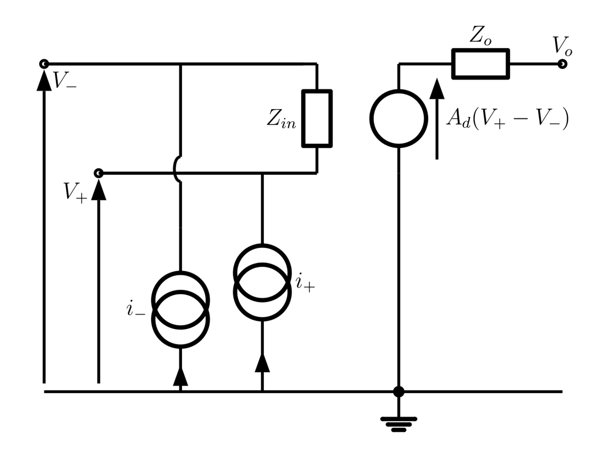
In the inverting amplifier shown below if the op-amp is ideal, $V_o$ will be at zero potential and the input currents $i_{-}$ and $i_{+}$ (shown in the equivalent circuit above) will also be zero. In practice this will not be true and the circuit produce an appreciable output offset voltage and input offset currents.
Experiment
Use the LM-741 op-amp as shown above (i.e. as an inverting amplifier with the input grounded). Use ±15 V supplies and choose $R_1 = 100\,\Omega$ and $R_2 = 1\, k\Omega$. Use the DVM to measure the dc output voltage $V_o$. As already noted, in an ideal situation this will be zero, but in this case, with a real op-amp, it will have a finite value. Try this out with a few (no more than 5) op-amps of identical type noting how the offset varies across the sample. This will give you an idea of what to expect when using commercial op-amps.
Using the equivalent circuit and assuming that apart from the input offset currents, the op-amp is ideal, estimate the value of $i_{-}$. Repeat this exercise with some other combinations of $R_1$ and $R_2$, maintaining the same ratio ($10\, k\Omega, ~100\, k\Omega$) and ($100\, k\Omega, ~1\, M\Omega$ ) and check that the results are consistent.
Show by measuring the output voltage that the offset can be reduced by connecting an appropriate value of resistor from the non-inverting terminal of the op-amp to ground. Repeat this measurement for the three different combinations of $R_1$ and $R_2$.