Thermal Design 3
PCB Design for Thermal Considerations.
Introduction
Modern power electronic devices and systems can handle significantly higher amount of power in smaller footprints, thanks to advances in semiconductors packaging technologies and system design techniques. Further to this we have seen higher processing power required for modern applications in digital integrated electronic circuits which demand significantly higher power. These all increase the density of power, which could lead to unwanted temperature increase. Please refer to lecture slides for more detailed examples. Therefore, understanding the thermal behaviour of electronic systems can help in the system design process. Since the heat is generated by electric power dissipation, hence detailed multi-physics modelling and analysis is required, which could significantly improve the performance and lifetime of these systems. Over the last lab/lecture sessions we practiced the equations, models and most importantly key rules of thumb (the application note provided by Texas Instrument) that govern temperature distribution in electronic systems. Hence, we learned how to choose appropriate components e.g. power transistors, design layout and add heatsink to presume the proposed electronic system will remain within the safe temperature margins. In this lab session students will learn how to model the thermal behaviour of a sample dc-dc converter.
Objectives:
- Export the mechanical model of PCB to ANSYS
- Determine the electrical power dissipation of key components and run Thermal Analysis
- Present the temperature distribution of the board
Lab Procedure
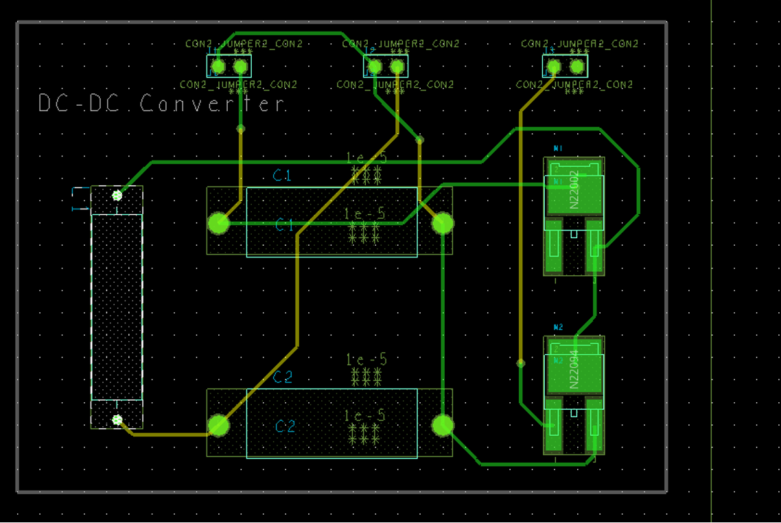
The PCB layout for DC-DC converter is provided in the previous labs as shown in .. The board file for this design is also uploaded on Moodle page of unit to allow students start from here.
This is a 2-dimensional layout file (2D), which contains information such as location of each component, its dimensions, connections (routes) etc. You may be able to generate a 3D image of this board in OrCAD environment. Depending on how much details provided in footprint library the 3D models appear closer to the real-life component . However, OrCAD uses the component outline to generate an approximate cubical shape around it, which is sufficient to start the thermal analysis.
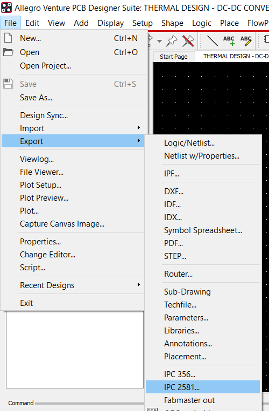
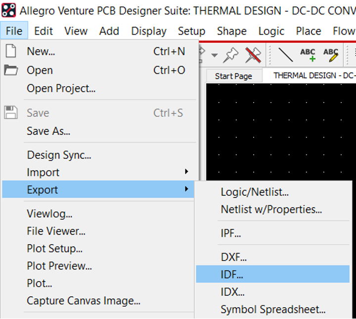
Two files must be exported from OrCAD Allegro to transfer the mechanical model of the PCB to other CAD tools and run thermal analysis.
- IPC2581
- IDF
Hence,
At this stage you have all the files required for implementing the mechanical model of PCB in ANSYS for following mechanical (thermal) simulations.
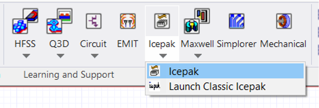
- Run ANSYS Electronics Desktop
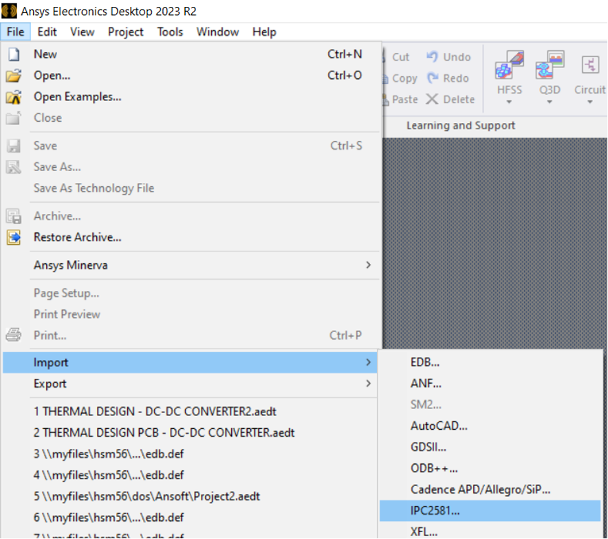
- From File menu select import IPC2581as shown below
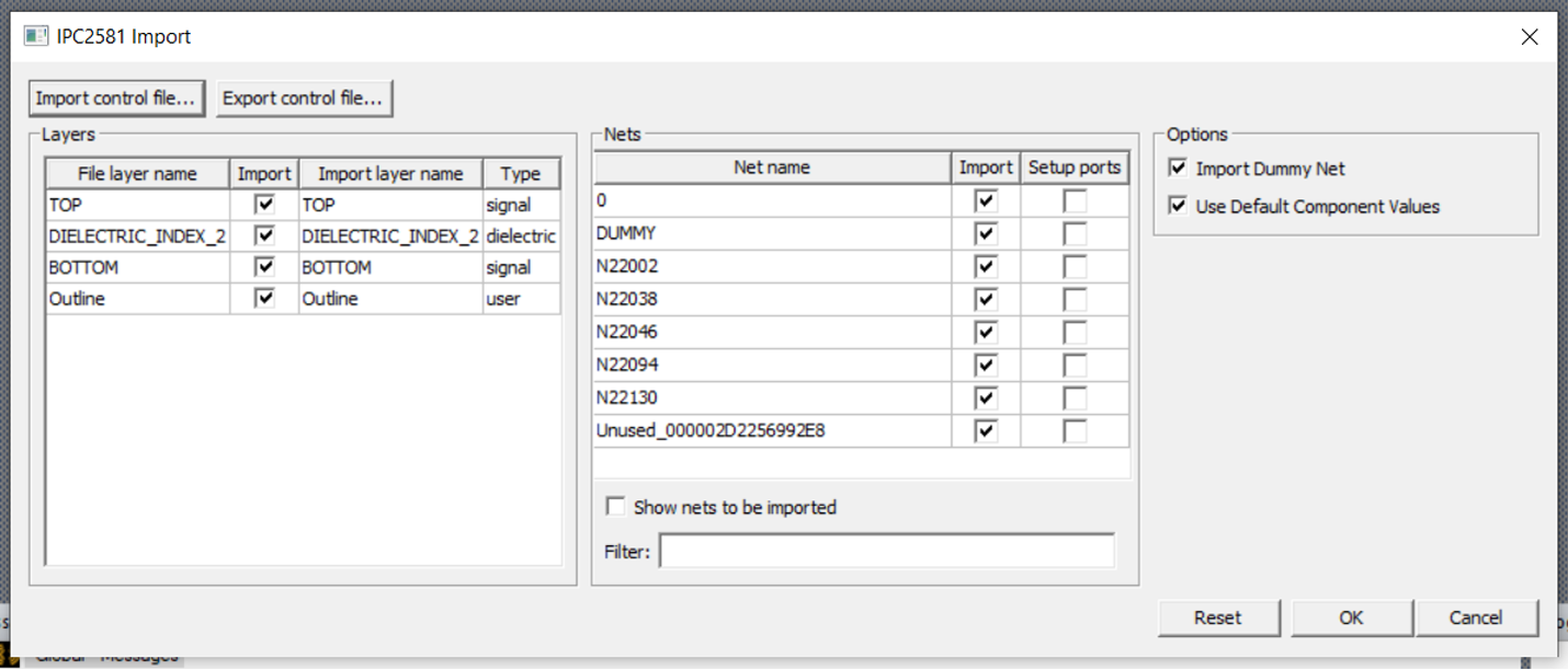
- The window shown in will appear, which confirms the layers of PCB included in the mechanical file. We have a simple two layer board hence the imported layers include top and bottom signal layers in addition to the dielectric and board outline.
Import layers
This is only a confirmation of the structure of imported board/components. For mechanical simulations we need the material properties to be confirmed as well.
- Make sure the
Desktopribbon is active (not View, Layout, etc) and Update material definitions
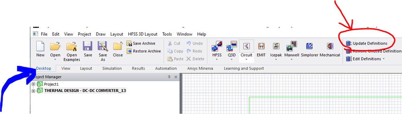
- Choose Update Definitions as shown in .
- After the following Window in appears, click on Show All Items
- This will fille in the Items List with the material outlined in (right-side),
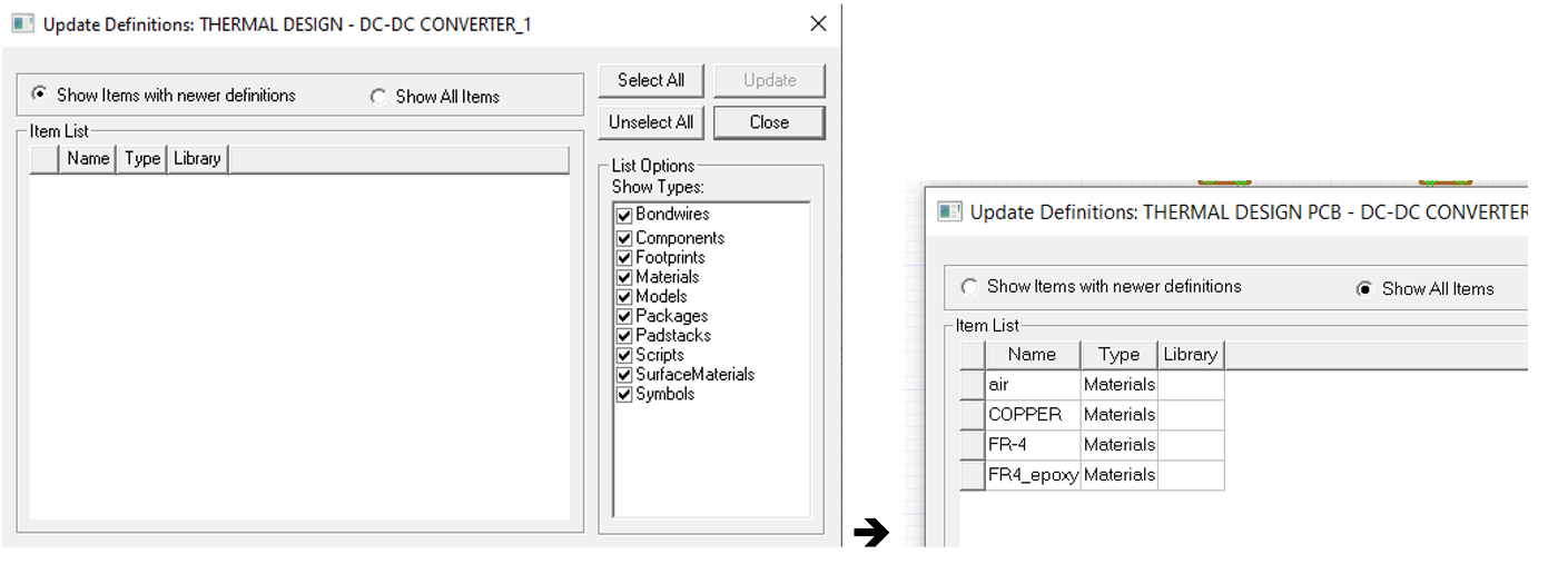
The fours listed material include Air surrounding the board required for cooling down the system, Copper of PCB traces, metal pads, and FR-4 as the board structural layer which is an electrical insulator but thermally conductive. This is obviously not the entire material included in the electronic system such as the metal pins of components, or ceramic and plastic material in components. Though this list is just enough to generate rough estimate of temperature distribution.
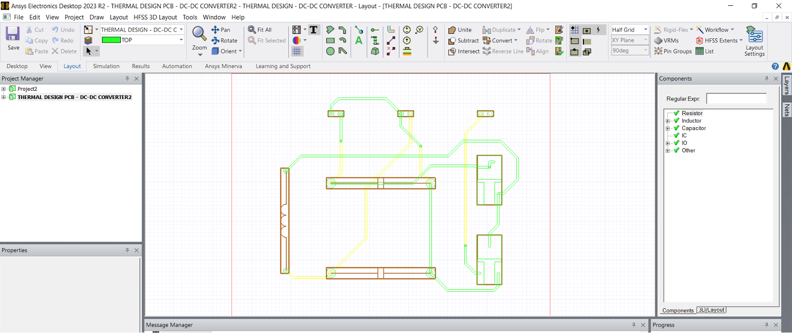
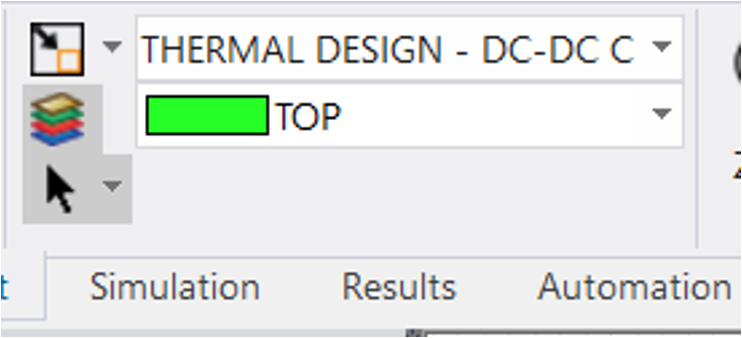
- At this stage switch to Layout ribbon and check the PCB layers imported from OrCAD layout by clicking on the icon shown below. This should show a one-to-one correspondence with the layers transferred from OrCAD PCB Editor.
At this stage we can regenerate a thermal model of PCB under IcePak.
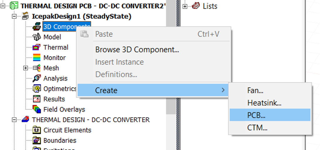
The setting window for PCB will appear as shown in . The first one only needs a few optional names.
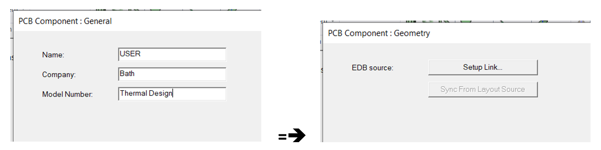
-
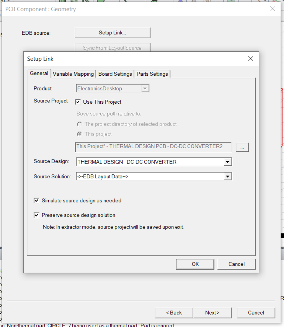
Click next and then setup link
-
Tick the box for
Use this projectas shown in , and let it self populate Check other boxes as shown below
- Under board setting change Air to FR4 and check the Use 3D layout box (under General)
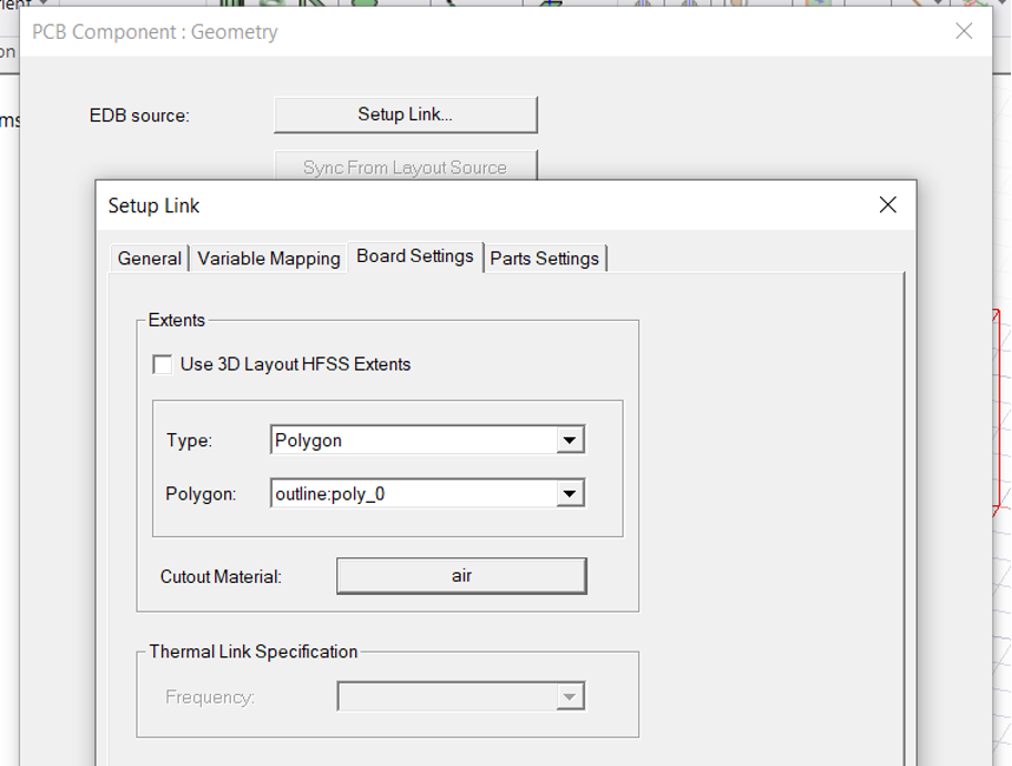
- Under part settings, Check
Device parts
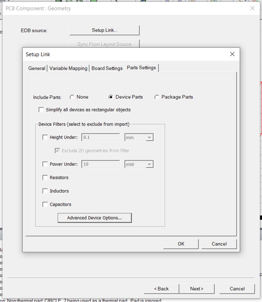
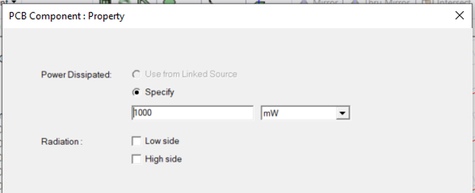
- Click OK and in the next step add
power.
-
Click
NextandFinish -
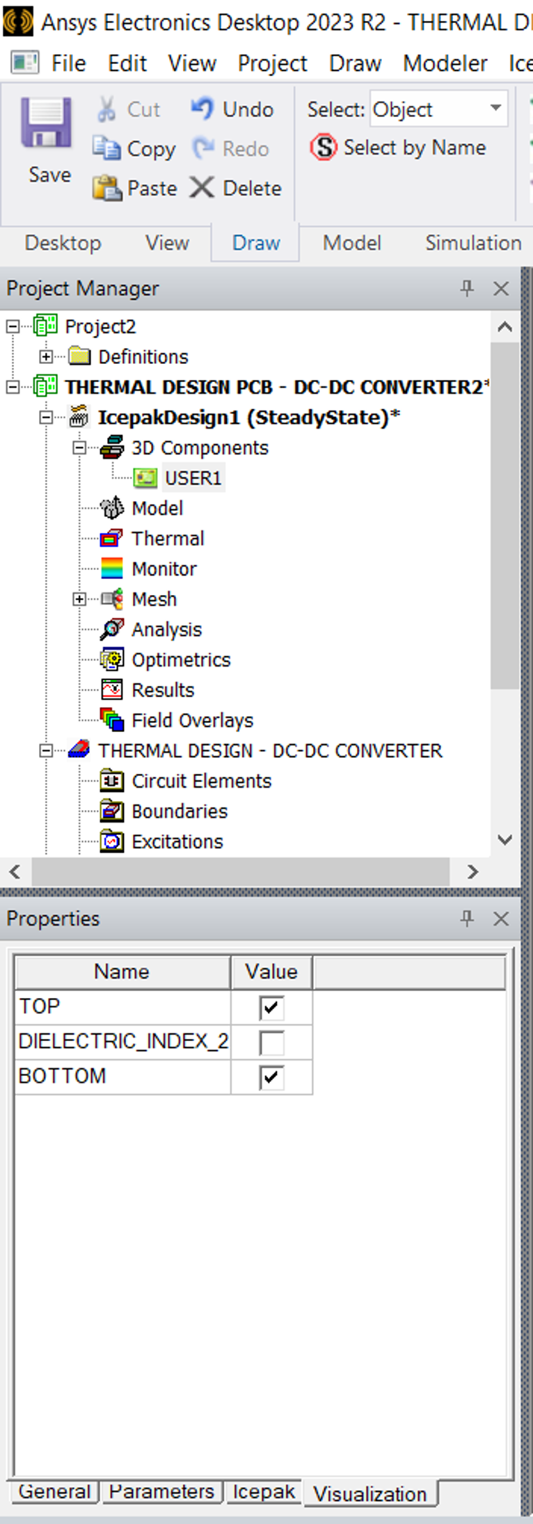
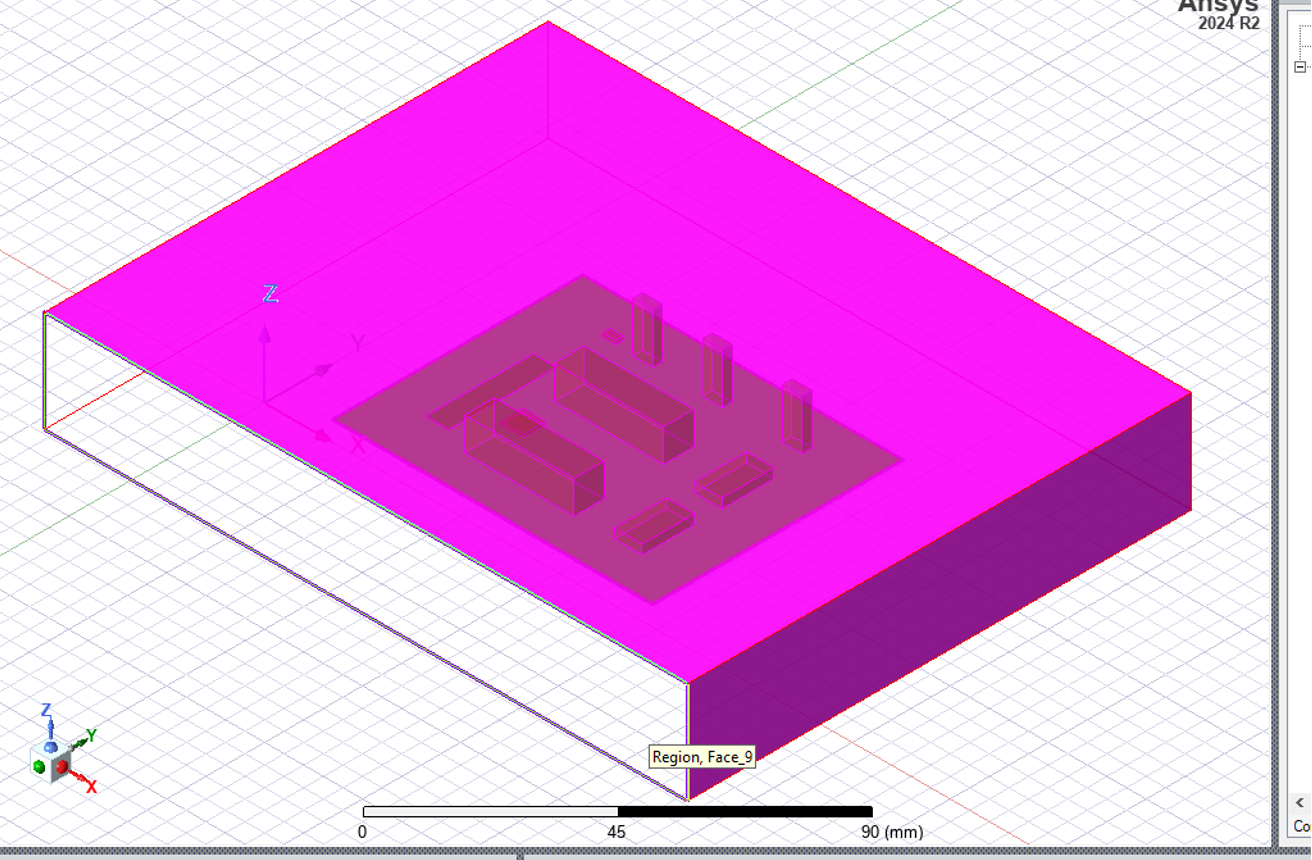
Select the PCB component from the project manager tree (or Model Tree) and under Visualization check the layers boxes to suit your preference this will allow you to see the tracks
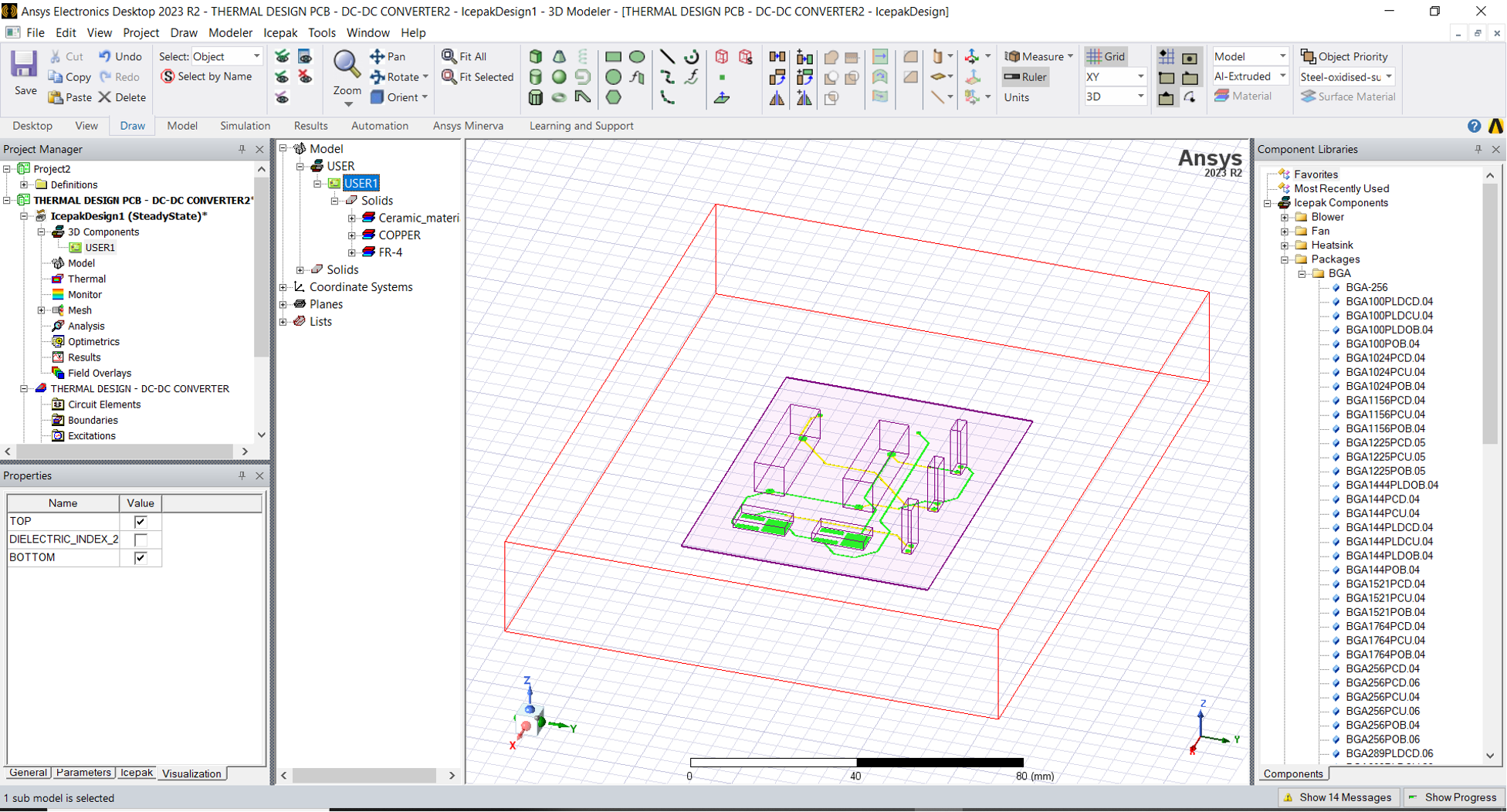
- Now right click on the PCB in the model tree and click fit in active view to see the PCB.
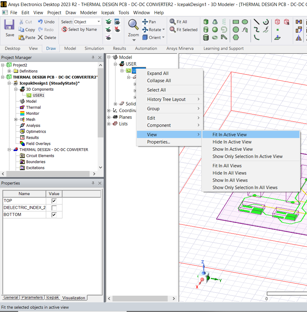
You should now have the view in the following image:
- Next
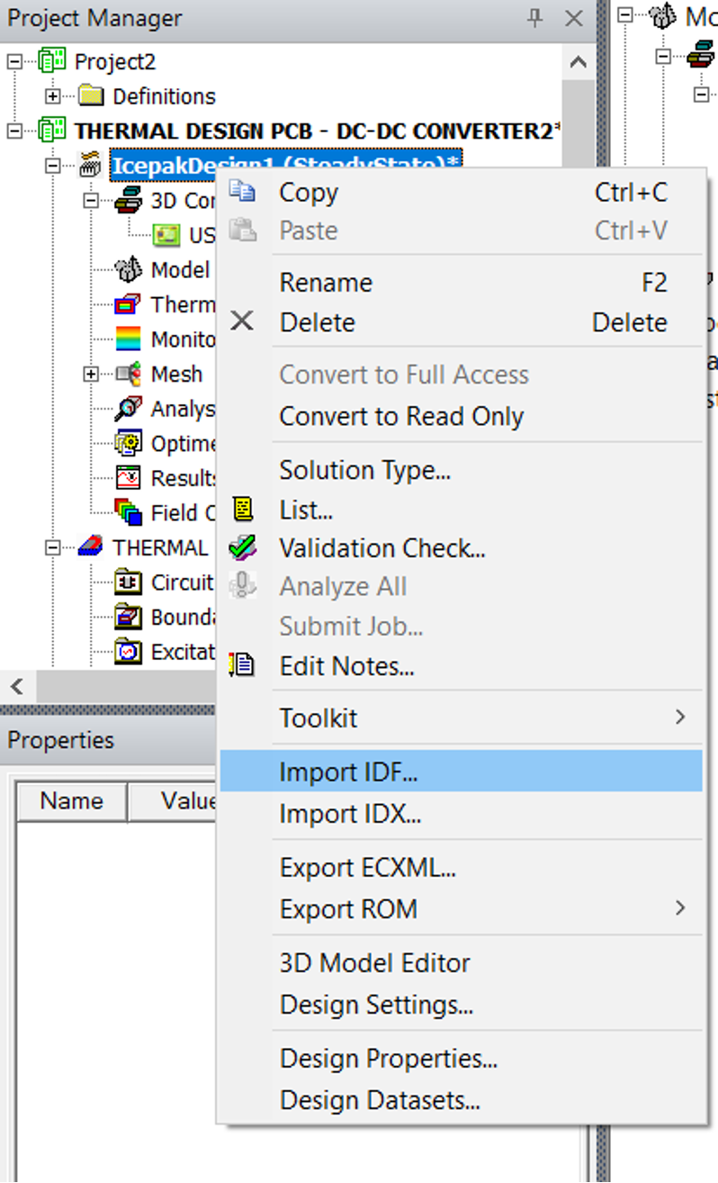
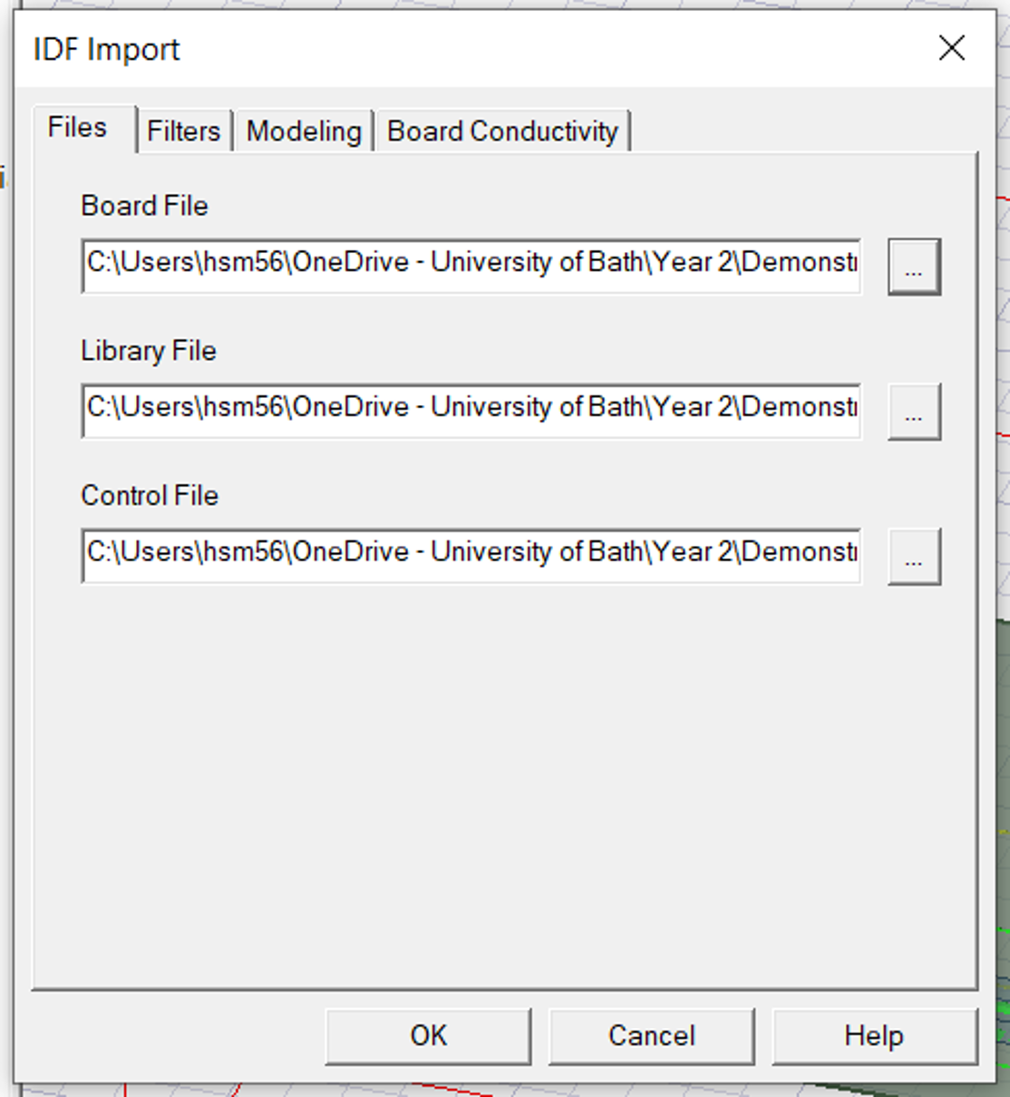
ImporttheIDFfile we exported from Cadence earlier by right clicking on theIcepakDesignas shown in .
- Select the correct files for all three below, in some cases, after selecting the Board File, the remaining two and auto selected as shown in .
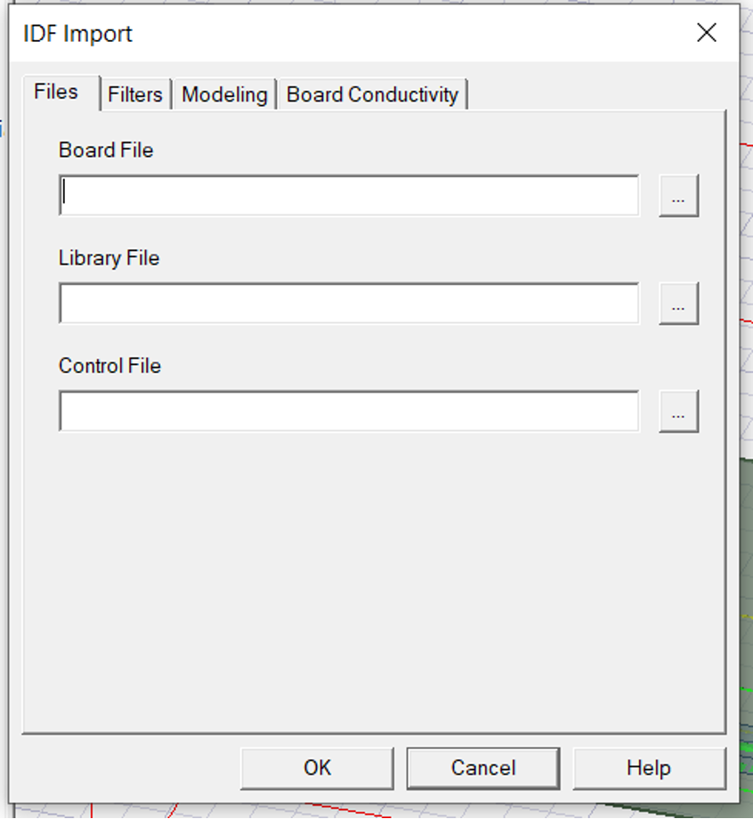
- Select the file with
.bdf extensionin the saved location asshown in . This is in Allegro folder wherever you have created the PCB layout next to the .brd file.

- Once all are filled click
OK.
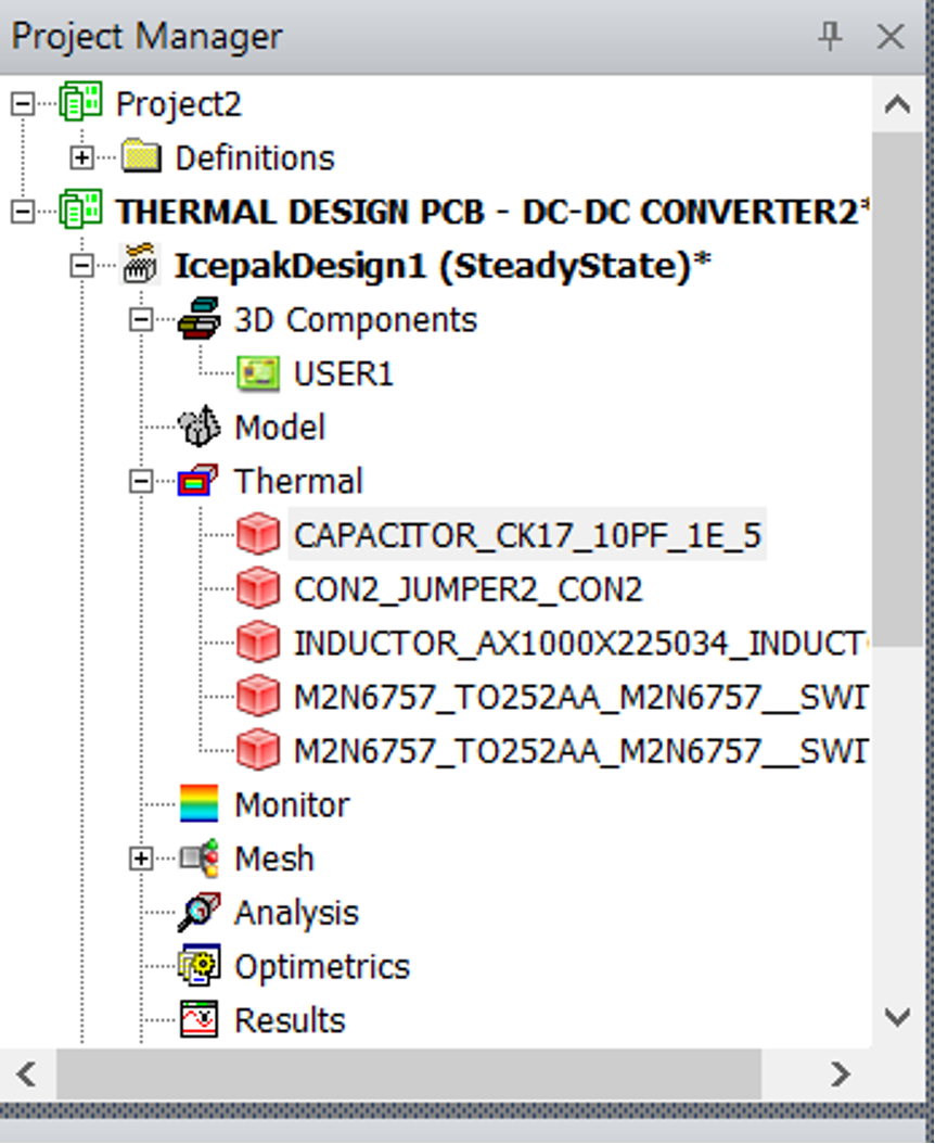
In the project manager you will see the thermal components created for PCB as shown in
Every finite element model requires a boundary condition. IN a not very accurate analogy this is similar to define ground node for simulation of electrical circuits. In the thermal context to solve the heat differential equation the solver require a initial condition to start with. It is easier to choose the air cube container of the model as the reference ambient temperature.
- Under
Editmenuselect SelectionMode and chooseFaces.
This will allow the user to choose faces by mouse click instead of components.
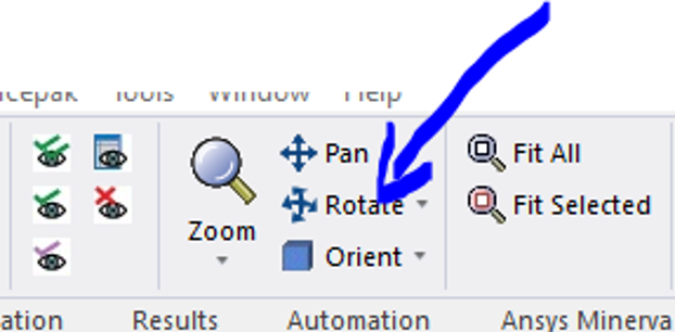
- Choose all the six faces of cube surrounding the PCB by pressing Ctrl and clicking on the faces as shown in .
- You will have access to one side of the model in the first view, hence to choose the surfaces at the back you may have to rotate the model using this tool
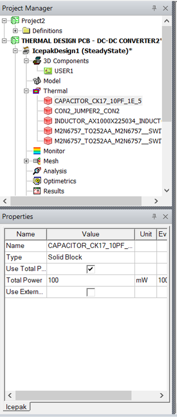
Flashback to the main DC-DC converter problem/project: we could assumed each transistor will dissipate around 5W (or whatever assumption you made) and the problem definition was to avoid hot points around capacitor, due to its restricted temperature rating.
- Assign
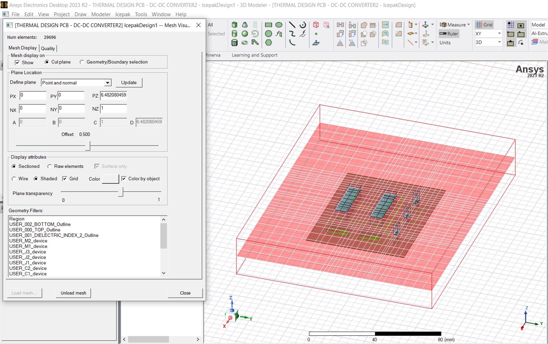
Mesh regionto PCB:
- In the Project manager tree under
Meshright click and then click onGenerate Mesh:
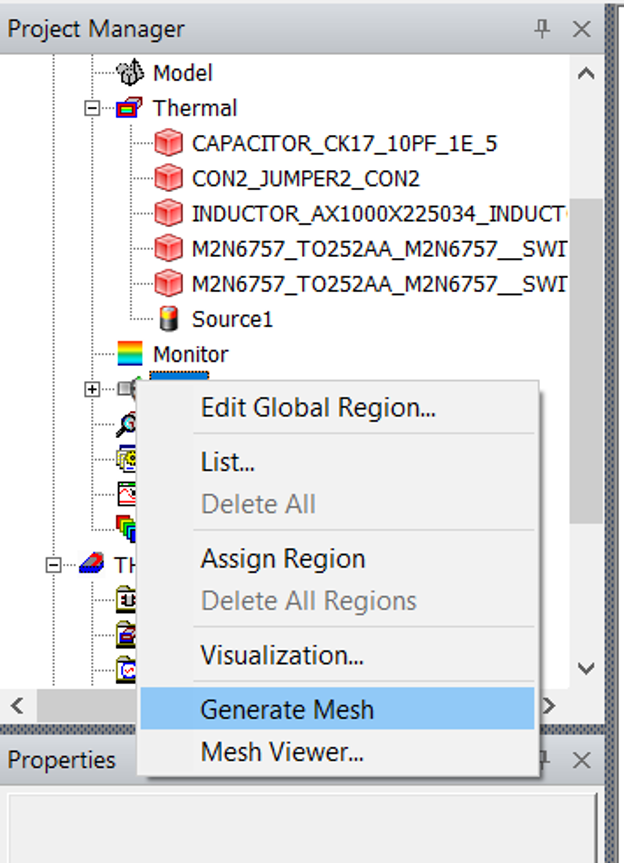
This will show a visualisation of the Mesh as per below:
- Now under
Analysis, right click and click onAdd solution Setup:
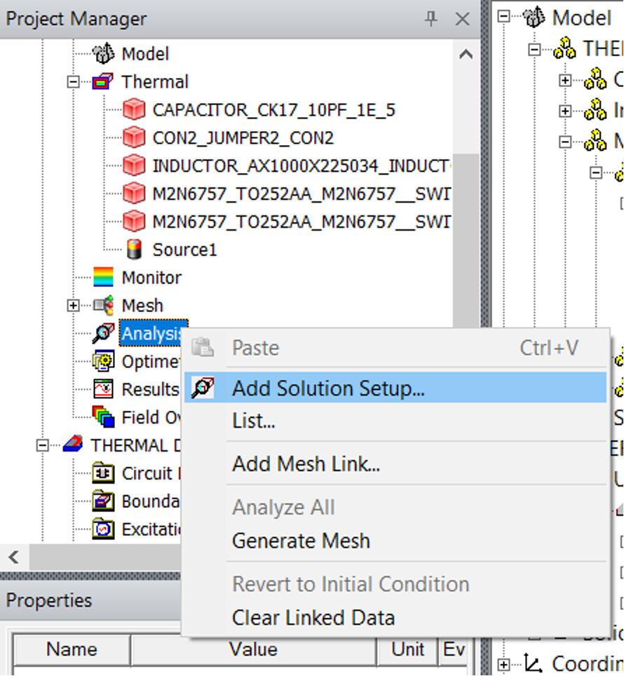
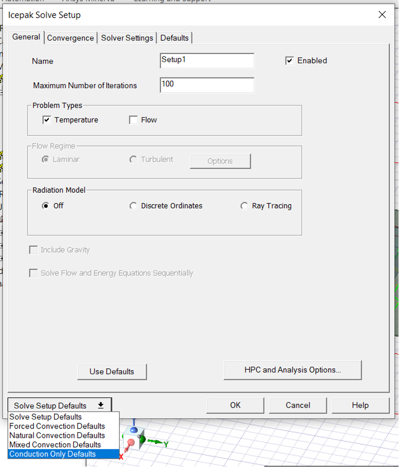
- Then choose
Conduction Onlydefaults from drop down menu and click on once all fields have been auto filled:
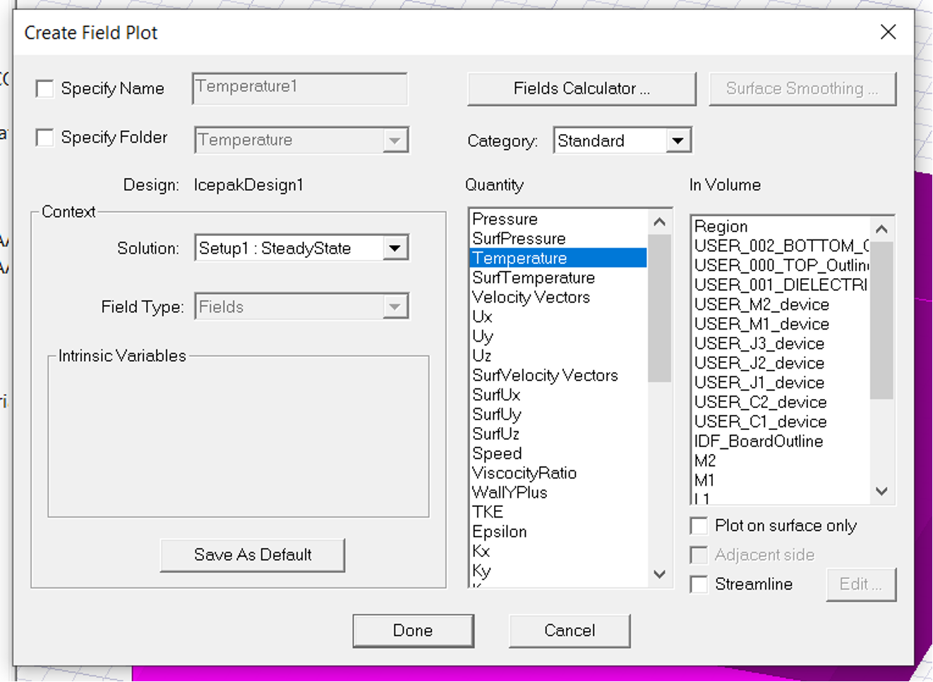
- Select the
PCBand then inField overlays, right click and selectTemperatureas shown:
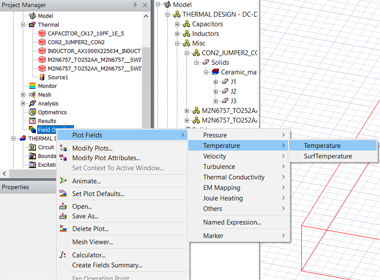
- This will bring up the below dialogue, select temperature and click Done:
- Now right click on
Analysisand clickAnalyze All
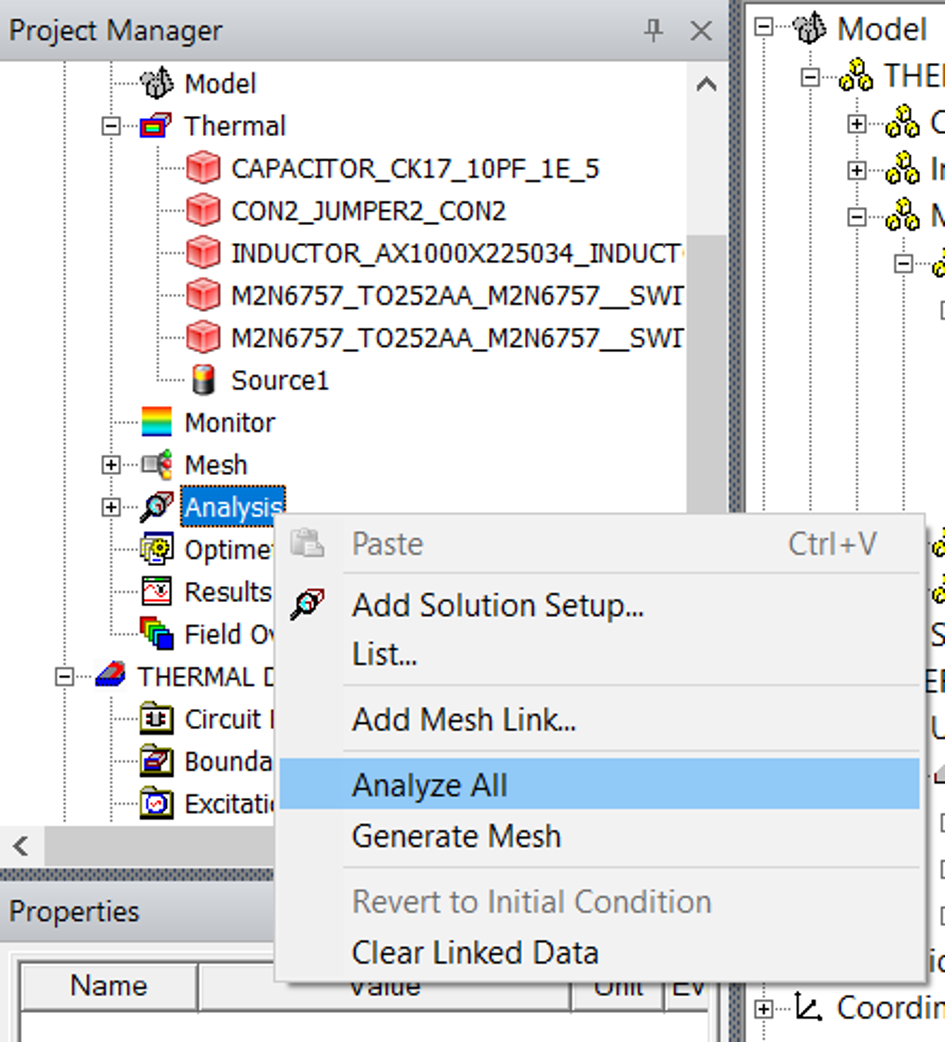
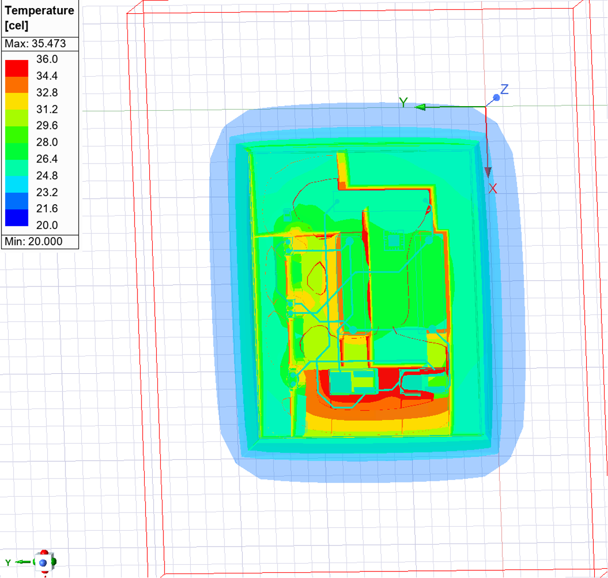
This should now Generate a temperature distribution plot as shown in .
Now that you have gone through the first round of modelling, the results will show you how close you are to the expected temperature distribution. Hence, if the results are far from expected margins the designer could go back to the original design and change the components or PCB design.