Power Electronics Simulation Lab
Introduction
In this lab we will simulate power electronics systems using free circuit simulation software, LTspice. In Section 1, we will go step-by-step through the simulation of a DC/DC Buck Converter to evaluate its performance. There will then be two exercises looking at Buck and Boost Converters. In Section 2, we will look at inverters and the differences between Square Wave, Quasi Square Wave and PWM-based inverters.
Preparation Work
- You can install LTSpice on your own computer by following the instructions here
- Look over the Power Electronics lectures and content from EE22004
Is the lab assessed?
The lab is associated with the Design Skill: “Power Electronics Simulation and Assessment”, which you should complete in your Mahara Portfolio.
Section 1: DC/DC Converters Walkthrough and Exercises
The first step in the lab is to create a model of the DC/DC Buck Converter using LTspice. This should be on all EEE lab computers or you can download and install it here.
Ensure that you save the design with a recognisable name (such as buck_converter) and save it regularly to avoid losing your work.
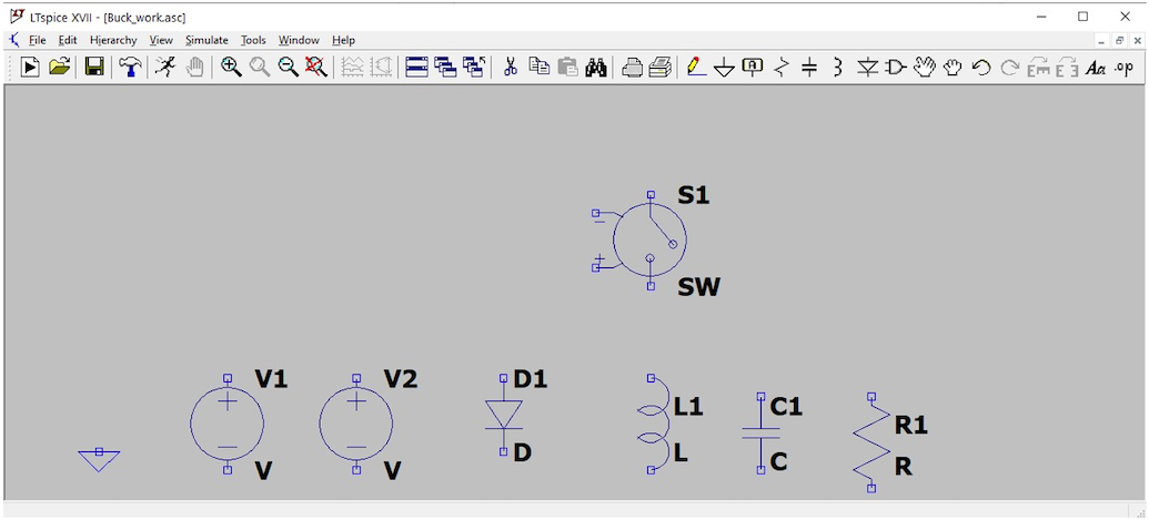
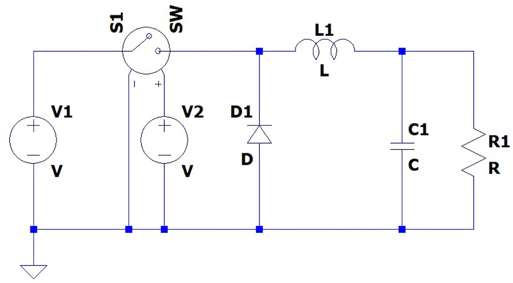
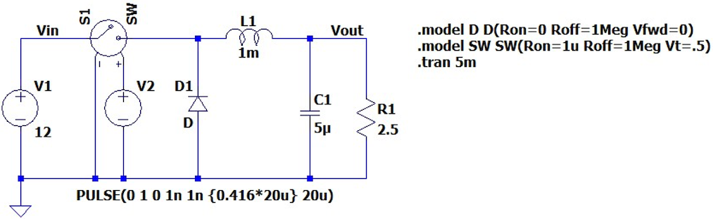
Once you have the schematic open (like in ), the first thing to do is obtain the components required for a Buck converter. You will need the following elements:
- Resistor (in the LTspice library this is called “res”)
- Capacitor (in the LTspice library this is called “cap”)
- Inductor (in the LTspice library this is called “ind”)
- Diode (in the LTspice library this is called “diode”)
- Switch (in the LTspice library this is called “sw”)
- Voltage Source (x2) (in the LTspice library this is called “voltage”)
- Ground (from the menu bar or by pressing “G” as it is not in the libraries)
Once you have all the components on the schematic, you should have something like .
You now need to arrange the components into the topology for a buck converter. You will find more details about the buck converter in Lecture notes on Moodle.
The basic topology of the Buck converter is shown in .
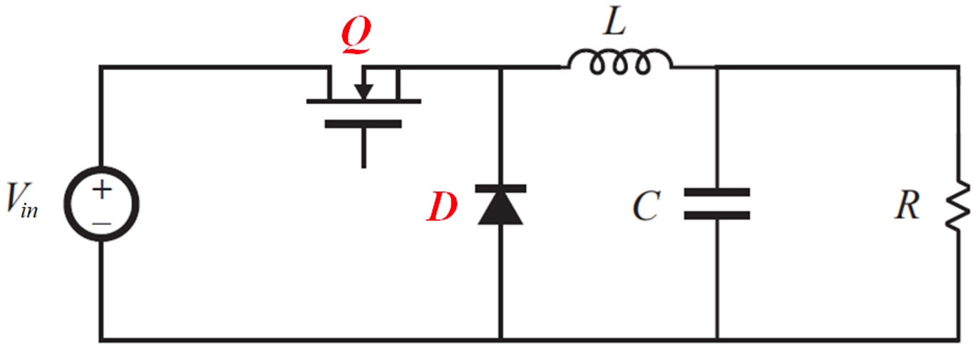
Go ahead and arrange the components from the ones you placed to match this topology until you have something like that in .
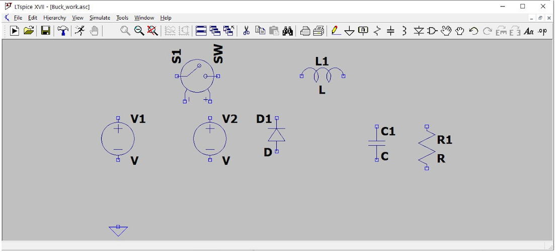
Once you have placed the components, connect them together, again as shown in .
Now we need to define the component parameters for the passive components, the input voltage source and the pulse generator.
The specification for the design is as follows:
| Specification | Value |
|---|---|
| Input Voltage | 12 V |
| Output Voltage | 5 V |
| Output Current (nominal) | 2 A (10W Power) |
| Inductor Current Ripple | 0.1 A |
| Output Voltage Ripple | 50 mV |
| Switching Frequency | 50 kHz |
Using the design equations defined in the notes for Lecture 2 of the Section on Power Electronics in EE22004, we can establish that the duty ratio, $D$, for the buck converter to achieve a 5 V output for a 12 V input voltage is as follows:
\[D = \frac{V_{out}}{V_{in}}\]Therefore, with these values, the resulting nominal duty ratio will be $D = 0.416$.
Nominal Duty Ratio = 0.416
At the switching frequency of 50 kHz, the inductance can be calculated using the equation for $\Delta I$ with the on time the duty ratio multiplied by the switching period. Assuming steady state, the input voltage will be 12 V and the output voltage 5 V:
\[L \ge \frac{(V_{in} - V_{out}) \times D}{\Delta I \times f_s}\]Using the specification values, this results in a minimum value of inductance of 582.4 µH. Normally we would specify the inductance above this to ensure that the ripple current is well below the specification, so let’s choose a value of 1 mH.
Value for Inductor 1 mH
Using the same equation (but solving for the ripple current), will give an estimated ripple current of:
Ripple Current: 58.24 mA
This is well below the specification limit of 100 mA, so even with a tolerance of 10-20%, we should still be well within our specification value (you can test this using the equations above if you are designing your own power converter to ensure this is the case by using the worst case values).
The load resistor is obtained by using Ohm’s law and therefore with a nominal output voltage of 5 V and current of 2 A, leads to a load resistor of 2.5 Ω.
Load Resistor = 2.5 Ω
While we have not explicitly discussed how to design the output capacitor for a specified voltage ripple (in practice it depends on the external control scheme which is beyond the scope of this course), a useful guideline equation can be used which is:
\[C out_{min} = \frac{\Delta I_L}{8 \times f_s \times \Delta V_{out}}\]In this design, the switching frequency ($f_s$) is 50 kHz, the ripple current is 58.24 mA, and the output voltage ripple has been specified as 50 mV. Using these values, we get a minimum output capacitance of 2.9 µF, which we can round up to a larger practical number, such as 3 µF or 5 µF to ensure that the output voltage ripple is within our specification.
Choosing a value of 5 µF should (using the equation above) give a maximum output voltage ripple of approximately 30 mV, however the simulated value might be somewhat lower than this in practice as this is simply a ballpark estimation of a minimum value for the capacitance.
You can always refine the value post simulation.
Output Capacitor = 5 µF
The next step is to modify the inductor, capacitor and resistor component values to these designed values on the schematic (you can leave the other parameter values in these components as their defaults for now).
At this point you can also change the input voltage source to its nominal value of 12 V.
Input Voltage Source = 12 V
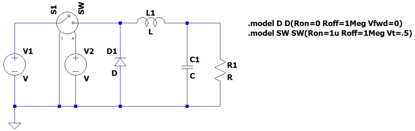
The next stage is to change some of the default parameters in the diode and switch components. These require us to define a model statement. This is achieved using the spice directive which is simply a text definition of a specific model parameter set for use by our components. We will need a model definition for the switch and the diode components.
The default diode is defined as a typical silicon diode, with a forward voltage of around 0.7 V. The on-voltage needs to be reduced otherwise this will reduce the output voltage (although the model for an realistic power diode (Schottky) might have a forward voltage of more like 0.3 V, I suggest changing it to 0 V as this exercise is assuming an ideal model – or at least very close to an ideal diode), and we need to change the on resistance to a much lower value to make the component behave more like an ideal diode. Change the Diode on resistance to 0 Ω. We also need a large off resistance, I suggest using 1 MΩ.
The default diode model has a model name of “D”, so we need to create a specific diode parameter set using this name (we could customise this and create our own name if we wished).
In the spice directive form, write the following text:
.model D D(Ron=0 Roff=1Meg Vfwd=0)This will create an ideal diode with the forward voltage of 0 V, an on resistance of 0 Ω.
- Diode On Resistance = 0 Ω
- Diode Forward Voltage = 0 V
- Diode Off Resistance = 1 MΩ
The switch on-resistance should also be set to a similarly low value, again suggested 1 mΩ.
The schematic should now have this additional text directive on the schematic. Note that this is NOT text, but a simulation command. Make sure that you have not added this as nonfunctional text.
We also need to add a similar model for the switch. The same on resistance and off resistance parameters will be required, however in the case of the switch, if we try and use an on resistance of 0 Ω the simulation will not converge, therefore we need to make this a small value, say 1 µΩ, to minimise the voltage drop across the device. Finally, we need to define the threshold at which the switch will change state, set this to 0.5V (we will use a 1V pulse to drive the switch – this is explained later in this section, where we will define the pulse source).
- Switch On Resistance = 1 µΩ
- Switch Off Resistance = 1 MΩ
- Switch threshold = 0.5 V
The spice directive needs to be:
.model SW SW(Ron=1u Roff=1Meg Vt=.5) The modified schematic will now look like .
The final model to define is the pulse generator. We need to define the switching frequency (50 kHz) and the duty ratio (0.416).
We have defined the switch component threshold is 0.5, and therefore the default amplitude of 1 will be fine for the pulse amplitude. The pulse generator requires the period rather than the frequency, therefore define the period using the inverse of the frequency, which is a value of 20 us. The pulse width is defined as a percentage of the period, which is the duty ratio multiplied by 100, which in this case gives a value of 41.6%.
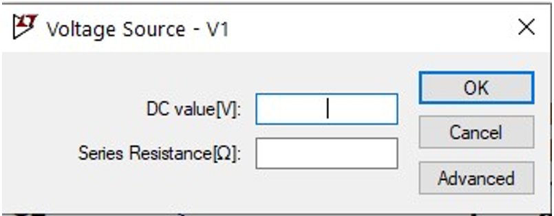
In order to define the pulse generator, when you edit the parameters for a voltage source it brings up the menu to define the DC voltage and Series resistance (see ), in order to change the behaviour to something more complex, we need to click on the advanced button.
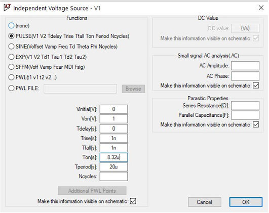
This will bring up the options for more advanced functions such as sine, pulse, pwl etc, as shown in . Select the Pulse option and you can then define the pulse drive characteristics.
- Initial Voltage = 0
- Von = 1
- Tdelay = 0
- Trise = 1n
- Tfall = 1n
- Tperiod = 20 us
- Ton = 41.6% = 8.32 us
The final setting is the end time of the simulation. We need to set this in the simulation directive once again, and this requires the spice directive as shown below to be added below the model definitions for the diode and the switch:
Simulation Stop Time = 5 msUse the following simulation directive in the same box as the model definitions:
.tran 5mMake sure you have changed the values of input voltage, inductance, capacitance, resistance on the schematic as per the values defined below:
| Component | Value |
|---|---|
| Inductor | 1m |
| Capacitor | 5u |
| Resistor | 2.5 |
| Input Voltage | 12 |
At this point you could run a simulation, however it is useful to label some of the voltages to observe what is going on, therefore go and label the input and output voltage nodes on the schematic, as shown in . The add label option is on the ribbon bar pf the LTSpice schematic interface, the F4 button (in Windows) or if you right click on the schematic window, under the “Draft” submenu you can add a label from there.
At this point you can run the simulation and if you click on the resistor (to plot the output current) and output voltage you can see the relevant waveforms which should look something like .
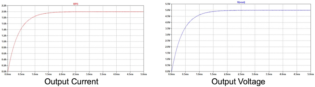
You can see from these figures that the average value of the output voltage is 5V and the nominal load current stabilises at a value of 2A.
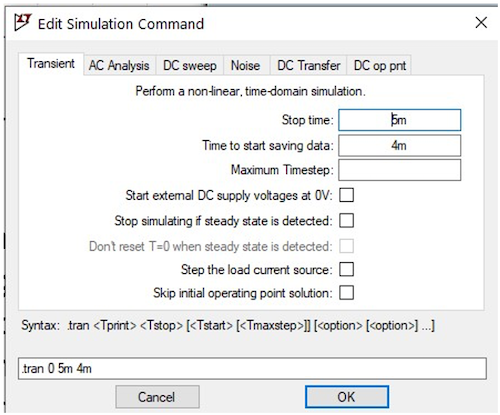
We can also carry out some post-processing to apply measurements to check specific parameters such as the average output voltage, output voltage ripple, average inductor current and also inductor current ripple. In order to do this, we can apply measurements to the waveforms. As we discussed in the lectures, these are defined when the DC/DC is operating in a steady state mode. If we look at the output voltage and current figures above, we can see that the waveforms stabilise in the final 2 ms of operation. Therefore, we can slightly modify the start time when the data will be stored. We can do this by specifying the start time in the command form, or by modifying the .tran command as shown in (in this case we will store data between 4 ms and 5 ms).
LTSpice has the option of adding measurement commands, and these include average and peak to peak measurements which are exactly what we need. These can be added to the simulation directive commands, and the results seen in the error log file, and there is another option which is to execute a measurement script (using the same commands).
In this instance we will show how to set up a separate measurement file.
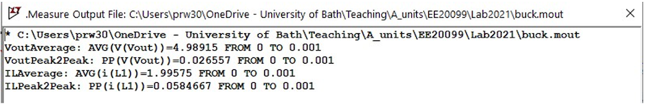
The first step is to create a blank text file – any text editor will do for this – and type in the following commands:
.MEAS TRAN VoutAverage AVG V(Vout)
.MEAS TRAN VoutPeak2Peak PP V(Vout)
.MEAS TRAN ILAverage AVG i(L1)
.MEAS TRAN ILPeak2Peak PP i(L1)If we take one of these commands we can break it down and see what each term means. If we start with the first command:
.MEAS TRAN VoutAverage AVG V(Vout)
- The first field is the measure keyword
.meas. This tells the software to carry out a measure. - The second field is the name of the analysis (
TRAN,ACetc) - The third field is the name of the result – we can use this to create composite measures for example.
- The fourth field (
AVG) is the measurement to be carried out (AVG= average,PP= Peak to Peak). You can find all the measurements in the LTSpice documentation. - The final and fifth field we have used is the signal to be measured. Notice that we have to specify voltage (
V(Vout)) or current (i(L1)) not just the name of the node.
Save this file with a .meas suffix (for example buck.meas) and then when the simulation has completed and you are looking at the results in a plot window, if you select the File → Execute .meas script function this can be used to load in your measurement script and this will calculate the values you have defined. The results of applying these measures to our circuit with the component values chosen result in the outputs shown in .
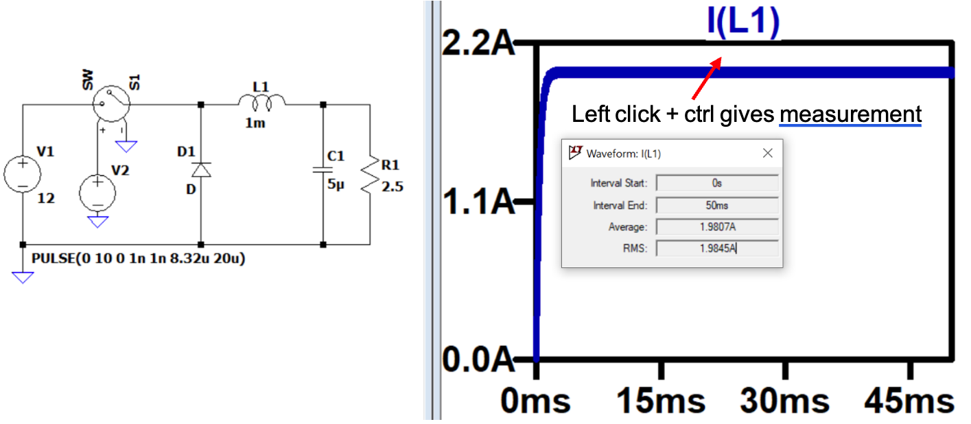
Note that we can also measure waveform values using the interactive waveform window – this has been demonstrated in lectures and can be achieved by zooming into the waveform section of interest and left-clicking the waveform name, while holding CTRL key, as shown in .
Looking at these results and comparing with our specification we can assess how well the design operates.
| Specification | Value | Measurement |
|---|---|---|
| Input Voltage | 12 V | |
| Output Voltage | 5 V | 4.989 V |
| Output Current (nominal) | 2 A (10W Power) | 1.996 A |
| Inductor Current Ripple | 0.1 A | 58.4 mA |
| Output Voltage Ripple | 50 mV | 26.6 mV |
| Switching Frequency | 50 kHz |
We can therefore say that this Buck converter meets our specification and is operating correctly.
As we noted above in our design process, in both the inductor and capacitor design steps, we chose values that ensured that our inductor current ripple and output voltage ripple were well above the limits in our specification, but what happens if we use the minimum values?
We can use the design in LTSpice to evaluate the minimum values of these components and find the limits using our model.
Starting with the inductance, we estimated that a value of 582.4 uH was the minimum inductance to meet our specification of inductor current ripple, therefore, if we change this value and rerun our simulations, we can measure what we obtain using this value:
| Specification | Value | Measurement |
|---|---|---|
| Input Voltage | 12 V | |
| Output Voltage | 5 V | 4.989 V |
| Output Current (nominal) | 2 A (10W Power) | 1.996 A |
| Inductor Current Ripple | 0.1 A | 100.4 mA |
| Output Voltage Ripple | 50 mV | 45.5 mV |
| Switching Frequency | 50 kHz |
This confirms that our estimated minimum value is almost exactly correct, and our design equation does provide a good estimate of the inductor ripple current.
It is also interesting to note that the output voltage ripple has increased (from about 25mV to 46mV), showing the direct relationship between the inductor current ripple and the output voltage ripple.
With the increased inductor ripple the minimum capacitance is 5 µF, and therefore our simulated value of 45.5mV is within 10% of the specification limit, and shows that our design equation is reasonable, although not quite as accurate as the inductor current ripple calculation.
Summary
We have seen how to create and run a simulation of a DC/DC Buck Converter model in LTSpice and to plot the results in also in LTSpice. We have also seen how to evaluate key performance metrics using the built-in measurement functions in LTSpice. This process can be used to analyse the fundamental performance of DC/DC converters.
Exercise 1 – Buck Converter
In the demonstration example design, the power converter was designed to convert from a 12 V battery to a 5V supply.
In this exercise, design a Buck DC/DC converter to convert a 9 V battery voltage to a 3.3 V logic system with the following specification:
| Specification | Value |
|---|---|
| Input Voltage | 9 V |
| Output Voltage | 3.3 V |
| Output Current (nominal) | 1 A (3.3W Power) |
| Inductor Current Ripple | 0.05 A |
| Output Voltage Ripple | 20 mV |
| Switching Frequency | 100 kHz |
Use the same design procedure as before and test the design using the schematic you created previously.
- Design the nominal duty ratio to obtain the correct output voltage
- Design the Minimum Inductance to achieve the required current ripple
- Design the nominal load resistance to achieve the target nominal output current
- Design the minimum Capacitance to achieve the required the output voltage ripple
| Parameter | Value |
|---|---|
| Minimum Inductance (uH) | |
| Minimum Capacitance (uF) | |
| Nominal Resistance (Ω) | |
| Nominal Duty Ratio (%) |
Exercise 2 – Boost Converter
In this exercise, design a Boost DC/DC converter to convert a 200V Photovoltaic Panel Array voltage to a 400 V DC Bus system with the following specification:
| Specification | Value |
|---|---|
| Input Voltage | 200 V |
| Output Voltage | 400 V |
| Output Current (nominal) | 2.5 A (1kW Power) |
| Inductor Current Ripple | 0.2 A |
| Output Voltage Ripple | 5 mV |
| Switching Frequency | 50 kHz |
Use a similar design procedure as before, however use the Boost converter equations from the notes and test the design using the new schematic.
Implement a new design with the topology you have chosen.
Design the values for the inductor, capacitor and resistor, and duty ratio to meet the specification as closely as possible.
| Parameter | Value |
|---|---|
| Minimum Inductance (uH) | |
| Minimum Capacitance (uF) | |
| Nominal Resistance (Ω) | |
| Nominal Duty Ratio (%) |
Section 2: Simulating and Comparing Inverter Types
Inverters, which convert DC to AC, are very widely used in power electronic systems (e.g. AC motor drives, UPS (uninterruptible power supplies), power-factor correction systems, and static var compensation systems) to synthesize AC waveforms. shows the connection of a 3-phase inverter in an AC motor drive. The inverter is used to vary the frequency and amplitude of the 3-phase output-voltage waveforms to allow the motor speed to be easily controlled.
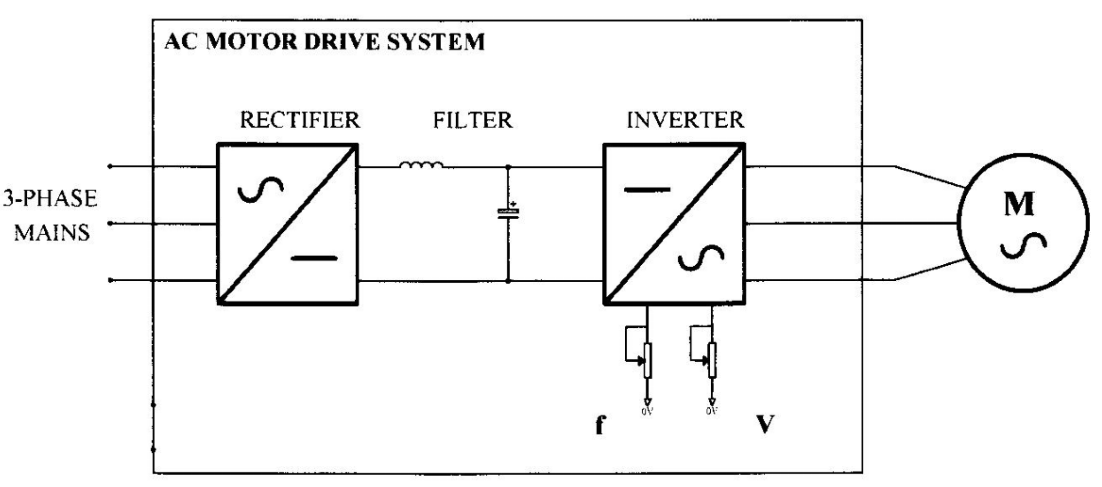
Inverters are often operated from an unregulated DC supply generated by rectifying and smoothing the AC mains voltage, as shown above. The inverter comprises a bridge of power-semiconductor devices, which are used in the switched-mode (i.e. switched between low-dissipation fully on and fully off states); and the output waveforms are usually synthesized using a form of pulse modulation, such as pulse-width modulation. The inverter therefore performs the function of a very efficient high-power amplifier. Inverters can be quite complex and there are several ways to control them. In this Section, we will compare Square Wave, Quasi-Square Wave and PWM Inverters – see Lecture 10 of the Power Electronics section of EE22004 as a reference.
Square Wave Inverter
We will first create a basic square wave inverter model in LTspice. We will use ideal switches instead of real devices and this will provide the basis for our exploration of the behaviour of the inverter using simulation.
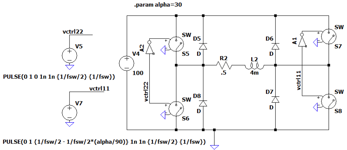
Create the LTSpice schematic shown in to simulate a square-wave inverter. The switches (SW) are switched between fully on and fully off, to produce unipolar anti-phase square-waves, VA and VB. The inductive load sees VO = VA-VB and thus an alternating, bipolar-voltage, square-wave output. The components for the switches, diodes, inductor and resistor and voltage sources are the same basic components as we used in the DC/DC converter lab.
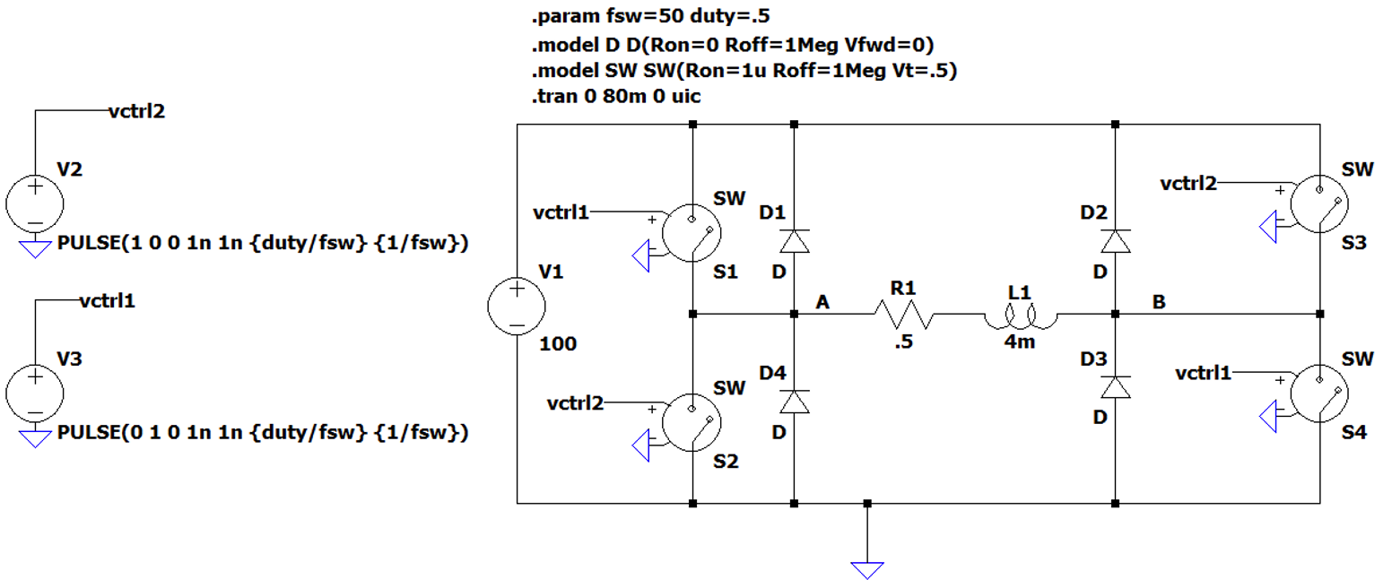
Here, we are also making use of simulation ‘Parameters’, where we can assign values to named variables an reuse them. This is done with the .param command to initialise the variable, and through using curly brackets {} to use the parameters in a circuit element. In the circuit above, we have the simulation command:
.param fsw 50 duty 0.5Which sets the switching frequency at 50 Hz and the duty cycle at 50%.
You can also plot algebraic expressions in LTspice by typing directly into the trace window, for example you could plot V(A)-V(B) or simply V(A,B) directly into the trace name and this automatically plots the differential output voltage without the need for the explicit voltage monitor circuit.
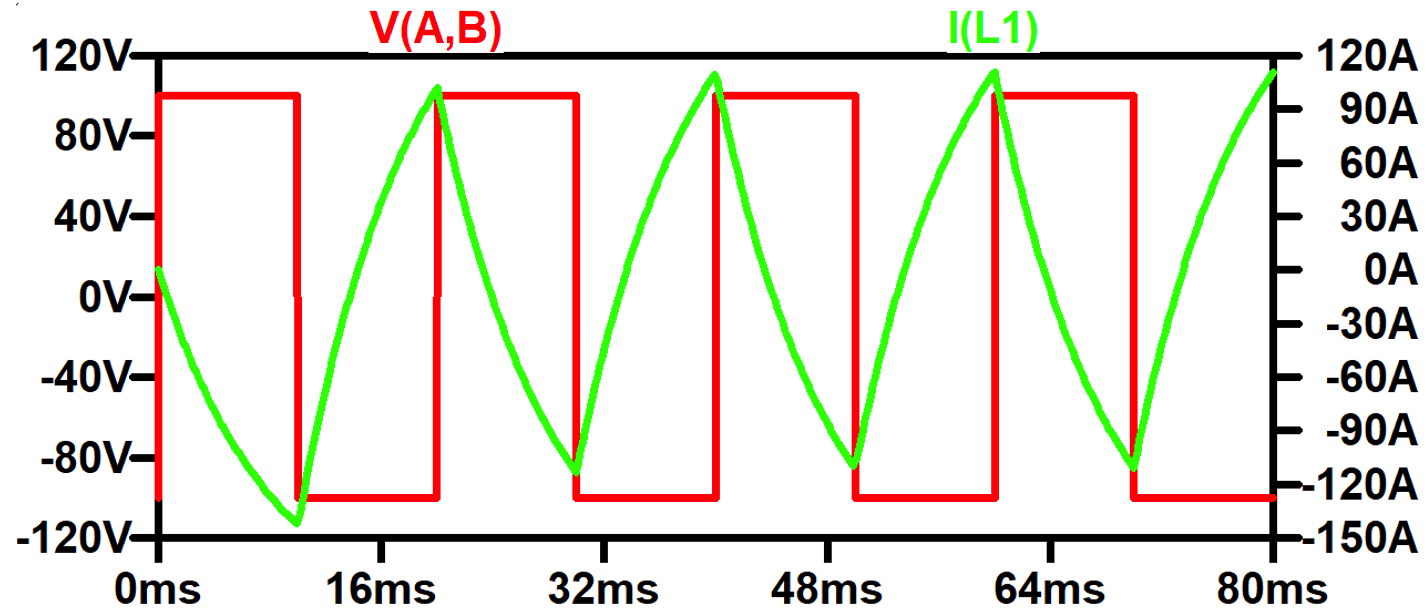
Even with the low-pass filtering effect of the inductive load, the output current is far from sinusoidal, and is generally inadequate to drive AC motors, for example, because the high harmonic-current content causes unacceptable torque ripple and motor heating.
We can perform a Fourier analysis of both the output voltage V(A,B) and inductor (output) current I(L1) to evaluate the harmonic performance of the inverter.
LTSpice has the ability to run a Fourier analysis on the data directly using the .four spice directive, therefore you can add this to the Spice Commands as follows:
.four 50 31 V(A,B)This command will run a Fourier on the signal V(A,B), with a fundamental frequency of 50 Hz and 31 harmonics (the default is 9).
Running this on the design in LTspice will show the harmonics in the Spice Log File, as shown in .
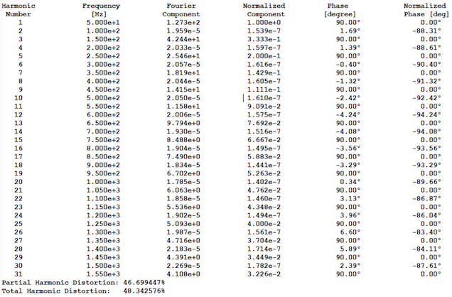
You can see from this table that the even harmonics are almost zero, and the odd harmonics have the majority of the content, as predicted by the theory. The Fourier analysis also calculates the total harmonic distortion of the waveform (THD) which is a good measure of the signal purity with respect to a sinusoidal waveform.
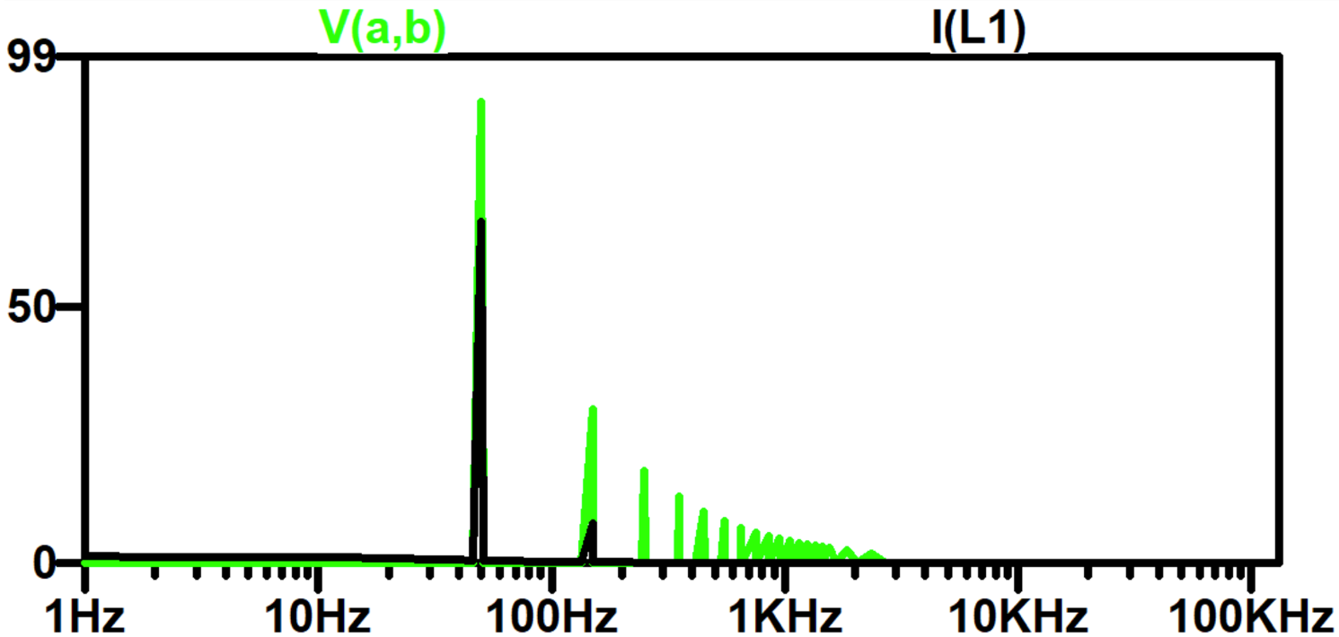
You can also plot the FFT spectra using the Show FFT command in the View menu of the waveform plot window. The default plots the dB values; however, you can right click on the Y-Axis and change to linear rather than dB. Looking at V(A,B), as shown in , we see the harmonic content and can also look at the harmonic content in the output I(L1), which is a filtered version of this and is quite sinusoidal.
Quasi-Square-Wave Inverter Operation
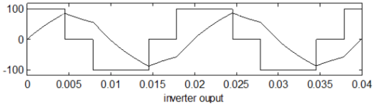
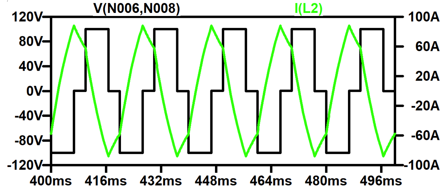
The output current waveform can be considerably improved by only switching the transistors on for 1/3 of the period rather than 1/2. This produces a stepped waveform called a quasi-square waveform, as in .
In order to create this quasi-square wave, we need to obtain a fraction of the pulse. There are several ways to do this, but the easiest is Phase Shift control, encountered in lectures and shown in . Recall that we can operate all 4 switches at 50% duty cycle, but shift the phase of one leg (left/right) with respect to the other. We introduce the switching angle, $\alpha$, where $\alpha=0$ means legs are out of phase and we get a 100% duty cycle, and $\alpha=90$, ($\frac{\pi}{2}$) means legs are in phase and we get 0% duty cycle.
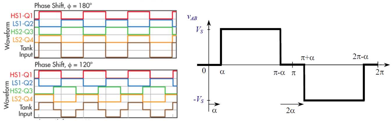
We can achieve this in several ways, with one way being to switch the top/bottom of each leg complementary using NOT gate and adding a delay between the legs based on alpha, as shown in .
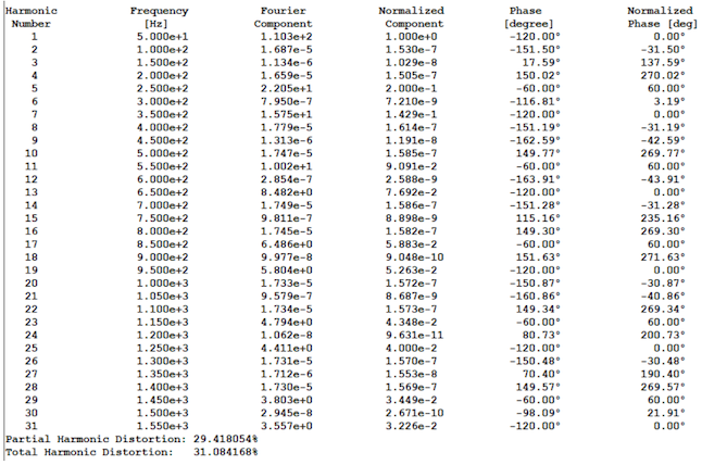
Running the simulation with $\alpha=30$ provides switch control waveforms with the characteristics shown in .
Running the FFT analysis as before, the THD reduces to 31% (down from over 48%), which is a significant reduction, as well as a complete elimination of the 3rd harmonic (as expected), as shown in .
PWM Inverter
The final option for improving the harmonics on the output are to use Pulse Width Modulation (PWM) of the output. In order to achieve this, it is necessary to modulate a reference with a triangular waveform, and to generate much higher frequency switching waveforms of the form shown in .
There are a number of ways to achieve this, in our case we take a triangle wave (cyan) and compare it to a reference sinusoid vref (green), to produce a PWM waveform (black) as shown in the schematic and waveforms in .
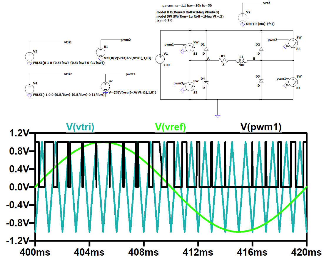
Running the simulation with a switching frequency set to 1 kHz, we get the waveform shown in .
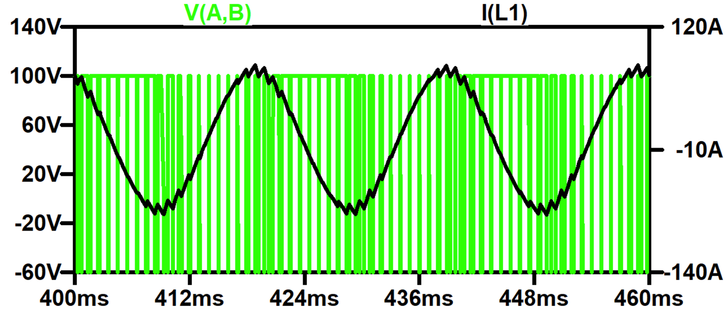
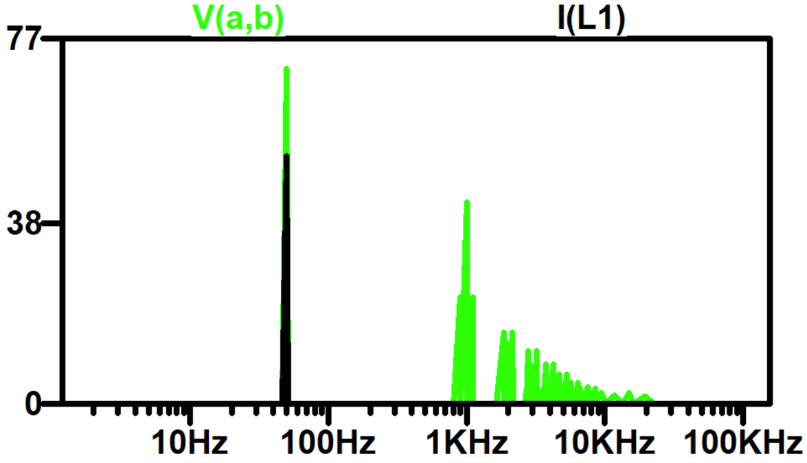
Looking at the FFT of the voltage and current shown in , we can see that V(A,B) has many higher harmonics, but importantly, these are at higher frequency, mainly around and above the switching frequency, so the load (which is an inductor) filters them out for a smooth, near-sinusoidal current.
Exercise – Inverter Comparisons
Using the square wave, quasi square wave and PWM inverters, run simulations with the following design criteria and measure the output characteristics as defined below.
Fundamental Design Parameters:
| Parameter | Value |
|---|---|
| Fundamental Frequency | 400 Hz |
| DC Link Voltage | 270 |
| Load Inductance | 1 mH |
| Load Resistance | 1.2 Ω |
| Switching Frequency | 12.8 kHz |
| Ma | 0.97 |
| Quasi Square On Time (adjust vth) | 33% |
Carry out the following Measurements with the Fourier Harmonics number set to 9 (default):
| Measurement | Square Wave | Quasi Square Wave | PWM |
|---|---|---|---|
| Load Current Fundamental (A) | 123.4 | 106.8 | 82.1 |
| Load Current 3rd Harmonic (A) | 15.1 | 0 | 13.9 |
| Load Current 5th Harmonic (A) | 5.51 | 4.7 | 4.3 |
| Load Voltage Fundamental (V) | 343.7 | 297.6 | 227.5 |
| Load Voltage 3rd Harmonic (V) | 114.6 | 0.1 | 105.6 |
| Load Voltage 5th Harmonic (V) | 68.7 | 59.6 | 53.2 |
| Load Current THD (%) | 13.26 | 4.6 | 17.86 |