Excitonic Solar cells
How do Excitonic cells work? Why Excitonic?
When a photon (a particle of light) is absorbed by the light-active component in an excitonic solar cell, a negatively charged electron is excited to higher energy. A positively charged hole is therefore also created on the molecule at the point where the electron is now absent. When the electron is initially excited it remains strongly bound to the hole due to typically low dielectric constants in organic semiconductors. This electron-hole pairing creates an excited state that behaves like a particle so we call it an exciton, giving these types of solar cells their name.
An interface between two different materials - an electron-transfer material that accepts the electrons and a hole-transport material that accepts the holes - is then needed to split the exciton into a separate electron and a hole. The electron and the hole can then separately migrate to different electrodes.
The charge separation of the negative charge and postive charges to different electrodes is crucial as it sets up an electrical potential (voltage). This drives a flow of electrons (current) round an outer circuit (that connects the two electrodes) where they can do some work, like power an electrical device. Once the electrons recombine with the hole at the other electrode, the system is reset and the whole process can be started again with another photon.
How do Perovskite cells work?
The active layer in perovskite cells consists of a semiconductor with the perovskite structure shown below for the widely used methyl ammonium lead iodide composition
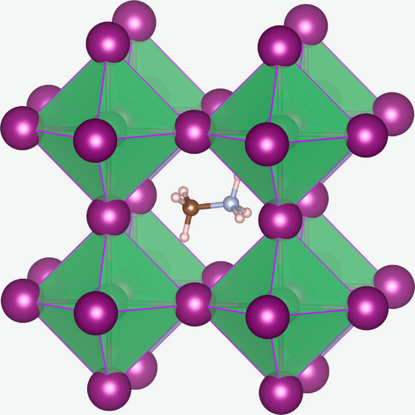
In this figure, taken from Eames et al Nature Comm 6 7497 (2015), the purple spheres are the iodide ions and the methyl ammonium is the organic molecule at the centre. The lead ions sit in the middle of the green octahedra.
A standard planar cell architecture is shown below (James Cave, 2017)
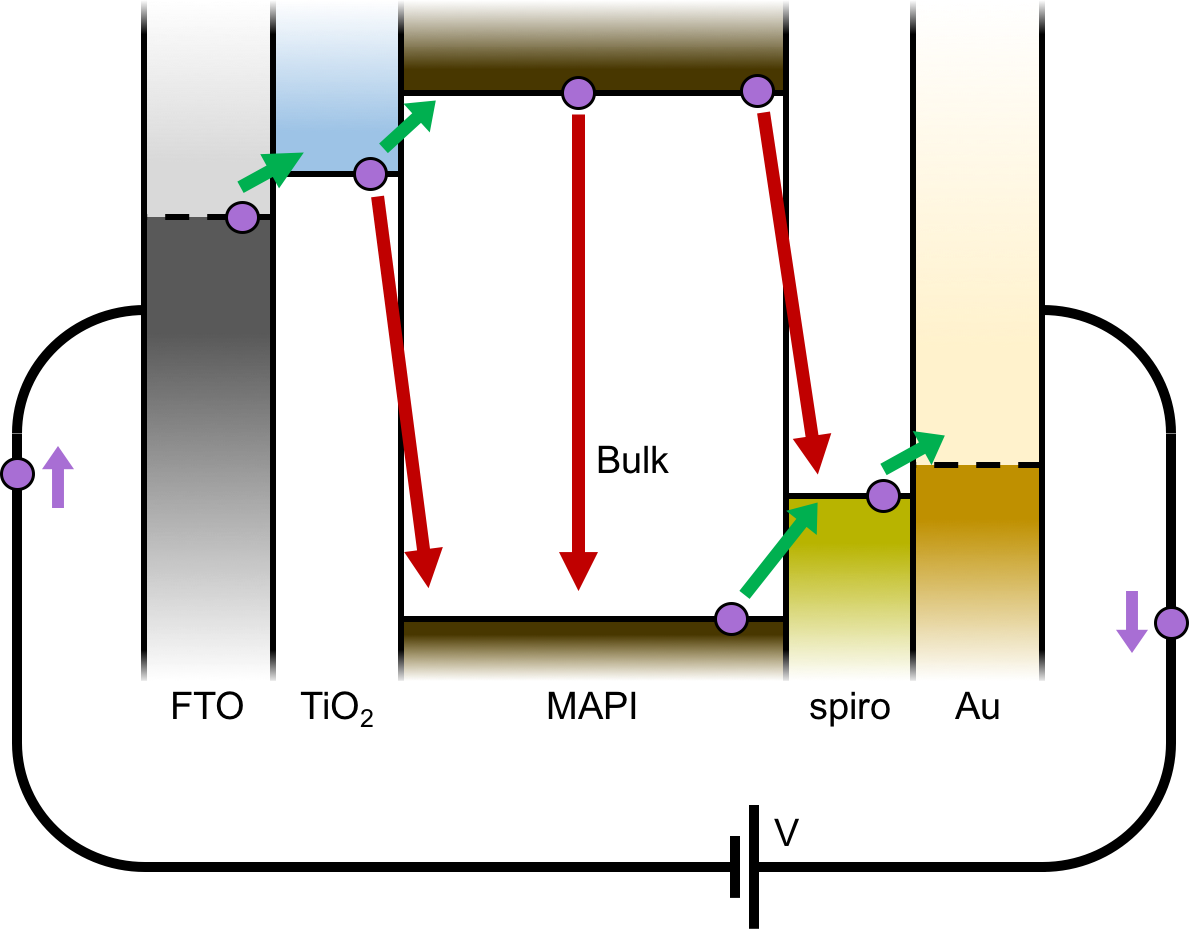
Light harvesting in perovskite cells takes place in the perovskite layers which are strong absorbers of incident solar radiation. The absorbed light excites electrons across the bandgap to create mobile electrons and holes that move towards respectively the electron transporting layer (TiO 2) and the hole transporting layer (spiro).
Holes leaving the Au contact re-enter the device via the fluorine doped tin oxide contact. The red arrows indicate recombination processes resulting in a loss of cell power efficiency are shown.
Perovskite and dye-sensitized cell Publications
-
Partial cation substitution reduces iodide ion transport in lead iodide perovskite solar cells
D W Ferdani, S R Pering, D Ghosh, P Kubiak, A B Walker, S E Lewis, A L Johnson, P Baker, M S Islam, P J Cameron,
Energy & Env Sci 12 2264 (2019)
-
Putting the Squeeze on Lead Iodide Perovskites: Pressure-Induced Effects To Tune Their Structural and Optoelectronic Behavior
D Ghosh, A Aziz, A B Walker, M S Islam
Chem Mat 31 4063 (2019)
-
How transport layer properties affect perovskite solar cell performance
N E Courtier, J M Cave, J M Foster, A B Walker, G Richardson
Energy & Env Sci 12 2264 (2019)
-
Systematic derivation of a surface polarisation model for planar perovskite solar cells
N E Courtier, J M Foster, S E J O'Kane, A B Walker
European J of Applied Maths 30 427 (2019)
-
Mixed A-Cation Perovskites for Solar Cells: Atomic-Scale Insights Into
Structural Distortion, Hydrogen Bonding, and Electronic Properties
D Ghosh, A R Smith, A B Walker, M S Islam
Chem Mat 30 5194 (2018)
-
Phase Behavior and Polymorphism of Formamidinium Lead Iodide
O J Weber, D Ghosh, S Gaines, P F Henry, A B Walker, M S Islam, M T Weller
Chem Mat 30 3768 (2018)
-
Lead-Free Perovskite Semiconductors Based on Germanium–Tin Solid Solutions
S Nagane, D Ghosh, R L Z Hoye, B Zhao, S Ahmad, A B Walker, M S Islam*, S Ogale, A Sadhanala
J Phys Chem C 122 5940 (2018)
-
Good Vibrations: Locking of Octahedral Tilting in Mixed-Cation Iodide Perovskites for Solar Cells
D Ghosh, P Walsh Atkins, M S Islam, A B Walker, C Eames
ACS Energy Letts 2 2424 (2017)
-
Azetidinium lead iodide for perovskite solar cells
S Pering, W Deng, J R Troughton, P Kubiak, D Ghosh, R Niemann, F Brivio, F Jeffrey, A B Walker, M S Islam, T Watson, P Raithby, A Johnson, S Lewis, P J Cameron
J Mater Chem A (2017)
-
Measurement and modelling of dark current decay transients in perovskite solar cells
S E J O’Kane, G Richardson, A Pockett, R G Niemann, J M Cave, N Sakai, G E Eperon, H J Snaith,
J M Foster, P J Cameron, A B Walker
J Mater Chem C
5 452 (2017)
-
Unconventional Thin Film Photovoltaics
Royal Society of Chemistry Energy and Environment Series (2016) Editors Enrico Da Como, Filippo De Angelis, Henry Snaith, Alison Walker including
Chapter on Modelling of Perovskite Solar Cells G Richardson, A B Walker
-
Can slow-moving ions explain hysteresis in the current-voltage curves of perovskite solar cells?
G Richardson, S E J O’Kane, R G Niemann, T A Peltola, J M Foster, P J Cameron, A B Walker
Energy & Env Sci (Open Access)
9 1476 (2016),
Electronic Supplementary Information
-
Characterization of Planar Lead Halide Perovskite Solar Cells by Impedance Spectroscopy, Open-Circuit Photovoltage Decay, and Intensity-Modulated Photovoltage/Photocurrent Spectroscopy
A Pockett, G Eperon, T A Peltola, H Snaith, A B Walker, L M Peter, P J Cameron, J Phys Chemistry C. 119 3456 (2015)
-
Influence of ionizing dopants on charge transport in organic semiconductors
A Abate, D R Staff, D J Hollmann, H J Snaith, A B Walker
Phys. Chem. Chem. Phys. 16 , 1132 (2014)
-
Structural and electronic properties of hybrid perovskites for high-efficiency thin-film photovoltaics from first-principles
F Brivio, A B Walker, A Walsh
APL Mat. 1 042111 (2013)
-
Monte Carlo Studies of Electronic Processes in Dye-Sensitized Solar Cells
A B Walker Invited review article
Springer Topics in Current Chemistry 2013
-
In Situ Detection of Free and Trapped Electrons in Dye-Sensitized Solar Cells by Photo-Induced Microwave Reflectance
H K Dunn,L M Peter, S J Bingham, E Maluta, A B Walker,
J. Phys. Chem. B, (2012) 116 , 22063
-
Determination of the electron diffusion length in dye-sensitized solar cells by substrate contact patterning
H K Dunn, P-O Westin, D R Staff, L M Peter, A B Walker, G Boschloo, A Hagfeldt
J. Phys. Chem. B, (2011) 115 ,13932
-
Real-time optical waveguide measurements of dye adsorption into nanocrystalline TiO2 films with relevance to dye-sensitized solar cellsA Peic,D R Staff,T Risbridger, B Menges,L M Peter, A B Walker, P J Cameron
J. Phys. Chem. B, (2011) 115 , 613
-
Dye-sensitized solar cells based on oriented TiO2 nanotube arrays: transport, trapping, and transfer of electrons
J R Jennings, A Ghicov, L M Peter, P Schmuki, A B Walker
J Am Chem Soc (2008) 130 13364
-
Transient photocurrents in dye-sensitized nanocrystalline solar cells
A B Walker, L M Peter, D Martinez, K Lobato Chimia (2007) 61 , 792
-
Analysis of photovoltage decay transients in dye-sensitized solar cells
A B Walker, L M Peter, K Lobato, P J Cameron J. Phys. Chem. B, (2006) 110 , 25504
-
Interpretation of apparent activation energies for electron transport in dye-sensitized nanocrystalline solar cells
L M Peter, A B Walker, G Boschloo, A Hagfeldt
J. Phys. Chem. B, (2006) 110 , 13694
-
Grain Morphology and Trapping Effects on Electron Transport in Dye-Sensitized Nanocrystalline Solar Cells
M J Cass, A B Walker, D Martinez, L M Peter
J. Phys. Chem. B, (2005) 109 , 5100
-
The distribution of photoinjected electrons in a dye-sensitized nanocrystalline TiO2 solar cell modelled by a boundary element method
F L Qiu, A C Fisher, A B Walker, L M Peter
Electrochemistry Communications (2003) 5 , 1388
-
Influence of grain morphology on electron transport in dye sensitized nanocrystalline solar cells
M J Cass, F L Qiu, A B Walker, A C Fisher, L M Peter
J. Phys. Chem. B (2003) 107 , 113
Microwave reflectance studies of photoelectrochemical kinetics at semiconductor electrodes
- 1. Steady-State, Transient, and Periodic Responses
M J Cass, N W Duffy, L M Peter, S R Pennock, S Ushiroda, A B Walker
J. Phys. Chem. B (2003) 107 , 5857
-
2. Hydrogen Evolution at p-Si in Ammonium Fluoride Solution
M J Cass, N W Duffy, L M Peter, S R Pennock, S Ushiroda, A B Walker
J. Phys. Chem. B (2003) 107 , 1520
-
Applications of microwave reflectance methods to the study of p-Si in fluoride solutions
M J Cass, N W Duffy, K Kirah, L M Peter, S R Pennock, S Ushiroda, A B Walker
J of Electroanal Chem (2002) 538-539 ,191
-
Electron transport in the dye sensitized nanocrystalline cell
A Kambili, A B Walker, F L Qiu, A C Fisher, A Savin, L M Peter
Physica E Low-Dimensional Systems & Nanostructures (2002) 14 , 203
|
Organic Devices
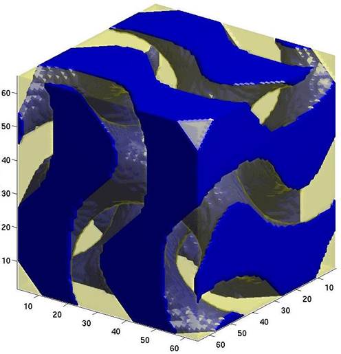
Rod morphology
 Disordered OPV blend model
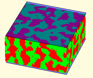 Gyroid morphology
Protein simulation publications
-
Salt bridge impact on global rigidity and thermostability in thermophilic citrate synthase
TJ McManus, S A Wells, A B Walker
Physical Biology (2019) Just accepted
Organic solar cell publications
-
Engineering two-phase and three-phase microstructures from water-based dispersions of nanoparticles for eco-friendly polymer solar cell applications
K Feron, J M Cave, M N Thameel, C O’Sullivan, R Kroon, M R. Andersson, X Zhou, C J Fell, W J Belcher, A B Walker, P C Dastoor
Chem Mater (2018) Just accepted
-
Utilizing Energy Transfer in Binary and Ternary Bulk Heterojunction Organic Solar Cells
K Feron, J M Cave, M N Thameel, C O’Sullivan, R Kroon, M R. Andersson, X Zhou, C J Fell, W J Belcher, A B Walker, P C Dastoor
ACS Appl. Mater. Interfaces (2016) 8 20928
-
Mesoscopic kinetic Monte Carlo modeling of organic photovoltaic device characteristics
R G E Kimber, E N Wright, S E J O'Kane, A B Walker, J C Blakesley
Phys Rev B (2012) 86, 235206
-
Simulation of loss mechanisms in organic solar cells
C Groves, R G E Kimber, A B Walker
J Chem Phys (2010) 133 , 144110
-
Bicontinuous minimal surface nanostructures for polymer blend solar cellsR G E Kimber, A B Walker, G E Schroder-Turk, D J Cleaver
Phys Chem Chem Phys (2010) 12 844
-
Dynamic Monte Carlo simulation for highly efficient polymer blend photovoltaics
L Y Meng, Y Shang, Q K Li, Y F Li, X W Zhan, Z G Shuai, R G E Kimber, A B Walker
J. Phys. Chem. B (2010) 114 , 36
-
Two-dimensional simulations of bulk heterojunction solar cell characteristics J H T Williams, A B Walker
Nanotechnology (2008) 19 , 424011
-
Dynamical Monte Carlo modelling of organic solar cells: The dependence of internal quantum efficiency on morphology P K Watkins, A B Walker, G L B Verschoor
Nano Letters (2005) 5 , 1814
Organic transport publications
-
Simulating morphologies of organic semiconductors by exploiting low-frequency vibrational modes
A R Smith, I R Thompson, A B Walker
J Chem Phys 150 164115 (2019)
-
Microscopic origins of charge transport in triphenylene systems
I R Thompson, M K Coe, A B Walker, M Ricci, O M Roscioni, C Zannoni
Phys Rev Materials (2018) 2 064601
-
Understanding The Role Of Ultra-Thin Polymeric Interlayers In Improving Efficiency Of Polymer Light Emitting Diodes
J Bailey, E N Wright, X Wang, A B Walker, D D C Bradley,J-S Kim
J Appl Phys (2014) 115 , 204508
-
Does supramolecular ordering influence exciton transport in conjugated systems? Insight from atomistic simulations
T A Papadopoulos, L Muccioli, S Athanasopoulos, A B Walker, C Zannoni, D Beljonne
Chemical Science (2011) 2 , 1025
-
Current-voltage characteristics of dendrimer light-emitting diodes
S G Stevenson, I D W Samuel, S V Staton, K A Knights, P L Burn, J H T Williams, A B WalkerJ Phys D: Applied Physics (2010) 43 , 385106
-
Exciton diffusion in energetically disordered organic materials
S Athanasopoulos, E V Emelianova, A B Walker, D Beljonne Phys Rev B (2009) 80 , 195209
-
Multiscale Modeling of Charge and Energy Transport in Organic Light-Emitting Diodes and Photovoltaics
A B Walker Proceedings of the IEEE (2009) 97 , 1587
-
Trap limited exciton transport in conjugated polymers
S Athanasopoulos, E Hennebicq, D Beljonne, A B Walker J Phys Chem C (2009) 112, 11532
-
Predictive study of charge transport in disordered semiconducting polymers
S Athanasopoulos, J Kirkpatrick, D Martinez, J M Frost, C M Foden, A B Walker, J Nelson Nano Lett (2007) 7, 1785
-
Electrical transport characteristics of single-layer organic devices from theory and experiment
S J Martin, A B Walker, A J Campbell, D D C Bradley
J Appl Phys (2005) 98 063709
-
Degradation in blue-emitting conjugated polymer diodes due to loss of ohmic hole injection
Appl Phys Lett (2004) 84 921
-
Effect of spatial irregularities on the temperature and field dependence of the mobility in liquid-crystalline conjugated polymer films S J Martin, A Kambili, A B Walker
Macromolecular Symposia (2004) 212 263
-
Temperature and field dependence of the mobility of highly ordered conjugated polymer films S J Martin, A Kambili, A B Walker
Phys Rev B (2003) 67 165214
-
Electrical transport modelling in organic electroluminescent devices A B Walker, S J Martin, A Kambili
J Phys Cond Matt Topical Review (2002) 14 9825
-
Modelling temperature-dependent current-voltage characteristics of an MEH-PPV organic light emitting device S J Martin, J M Lupton, I D W Samuel, A B Walker J Phys Cond Matt (2002) 14 9925
-
The internal electric field distribution in bilayer organic light emitting diodes S J Martin, G L B Verschoor, M A Webster, A B Walker Org El(2002) 3129
-
Transport properties of highly aligned polymer light-emitting diodes A Kambili, A B Walker Phys Rev B(2001) 6301129
|
Charge and energy transport models
Kinetic Monte Carlo, KMC, Method
KMC stochastically chooses events that occur based on how quickly that event can take place. The type of events that occur in our organic devices involve charge and exciton movement, charge injection (from electrodes) and exciton formation and recombination.
These simulations utilize a 3-dimensional user created morphology, and makes the model very versitile at exploring the effect different device structures and geometries have on device performance. This is coupled with the ability to view and track all particle species within the device through time.
Drift Diffusion Model
A drift diffusion model has been created to solve the transport equations in 1D for charge and energy movement within organic devices. The model is a quick way of testing new ideas, and an excellent tool to run alongside the KMC model.
Optical Model
In an optical model, Maxwell's equations are solved to predict the variations in field associated with the photons generated (OLEDs), incident (organic photovoltaics). The model allows us to deduce the efficiency and light intensity emitted from OLEDs or equivalently the external quantum efficiency and current-voltage characteristics produced by organic photovoltaics.
Research Goals
Using the KMC and Drift Diffusion models it is possible to investigate how different structures affect the positions of exciton dissociation and recombination zones. These charge and energy transport models can be applied to any devices employing organic semiconductors (OLEDS) and organic field effect transistors
(OFETS).
|