Research
Our research focuses on the heterogeneous integration of chemical vapour deposited aligned nanomaterials, engineered at the nanoscale, for functionally enhanced vacuum power electronics devices to realise next generation room temeprature operating, field electron emission based advanced computation devices and radiation sources for pulsed X-ray imaging and high-data rate communications transmission systems.
Interests
- Nanomaterial Growth
- Nanomaterial Alignement & Ultra-Precision Engineering
- Applied Nano Field Electron Emission
- Vacuum Power Electronics & Radiation (X-ray, THz) Sources
- Nanomaterial-based Bioelectronics
Research Projects
-
The underlying dispersive growth kinetics, and characterisation of thermal chemical vapour deposited (CVD) nanomaterials using foils, PVD thin films on Si and Si/SiO2, and non-catalytic thermal-CVD on GaN, and SiO2 is investigated. The heterogeneous catalysis of carbon nanotubes, synthesised by thermal and plasma enhanced chemical vapour deposition, is also studied using supergrowth Al2Ox/Fe bilayer and ITO/Ni dot array catalysts. Conditions for large-area, wafer-scale synthesis of monolayer graphene, single-wall CNTs and multi-wall CNTs for wafer-scale transfer and characterisation.
This research addresses the key challenges for technology up-scaling and pragmatic integration. Working with industry, we have developed catalyst structures and growth recipes for large area chemical vapour deposition of mono- and multi-layer graphene, MWCNTs and SWCNTs from R&D scale samples, as small as 5x5 mm, up to industry-scale 300 mm wafers using micro-CVD reactors and load-lock commercial systems.
-
Photonic crystals and metamaterials elicit a number of novel optical properties not found in nature. Understanding and developing protocols to achieve accurate alignment of CNTs,en masse, offers one possible route to fabricate such enigmatic materials. Here, we are principally concerned with dry-transfer techniques to preserve the anisotropic nanomaterials as-synthesised electronic structure. Here we research dielectrophoresis - based on anisotropic torque induction-, gas alignment, as well as solid-state extrusion, an effect attributed to high inter-tube van der Waals binding, with the optical properties of the resulting aligned, pseudo regular nanoscale materials investigated.
-
Field emission electron sources permeate health care, border control, and graphical user interface / display technologies. Field Emission is the liberation of electrons from an electron-dense solid into a vacuum, under the application of an intense electric field. It is a quantum mechanical phenomenon and can be succinctly described in adequate detail using fairly simplistic descriptors based on the free-electron model. A potential difference is applied between an electron emitting surface (cathode) and a counter electrode (anode). Electrons confined to the Fermi Sea Fowler-Nordheim tunnel through the electric-field-narrowed triangular potential barrier thereby producing collimated beams of electrons.
Graphitic nanocarbons, and graphene in particular, are low-Z materials and have one of the lowest secondary electron and backscattered electron yields reported to date, which in the case of graphene is a consequence of its linear dispersion. Subsequently, graphitic nanocarbons are near ideal electron emitters and electron transparent media. The energy barrier associated with atomic migration and surface diffusion is much larger than in metallic emitters, making CNTs highly stable. Similarly, the sp2 bonding in CNTs are significantly stronger than the metallic bonds of ubiquitous refractory metal electron emitter tips, allowing CNTs to carry current densities of up to 109 A/cm2 and the ability to withstand extremely intense electric fields (several V/nm) necessary for high current applications, specifically X-ray generators, with the CNTs remaining exceptionally stable at temperatures of up to 2000 K. CNTs are physically inert to sputtering and chemically inert to surface work-function adjusting absorbates. The combination of high temperature and high electric fields in metals induce field-sharpening by surface diffusion and electro migration.
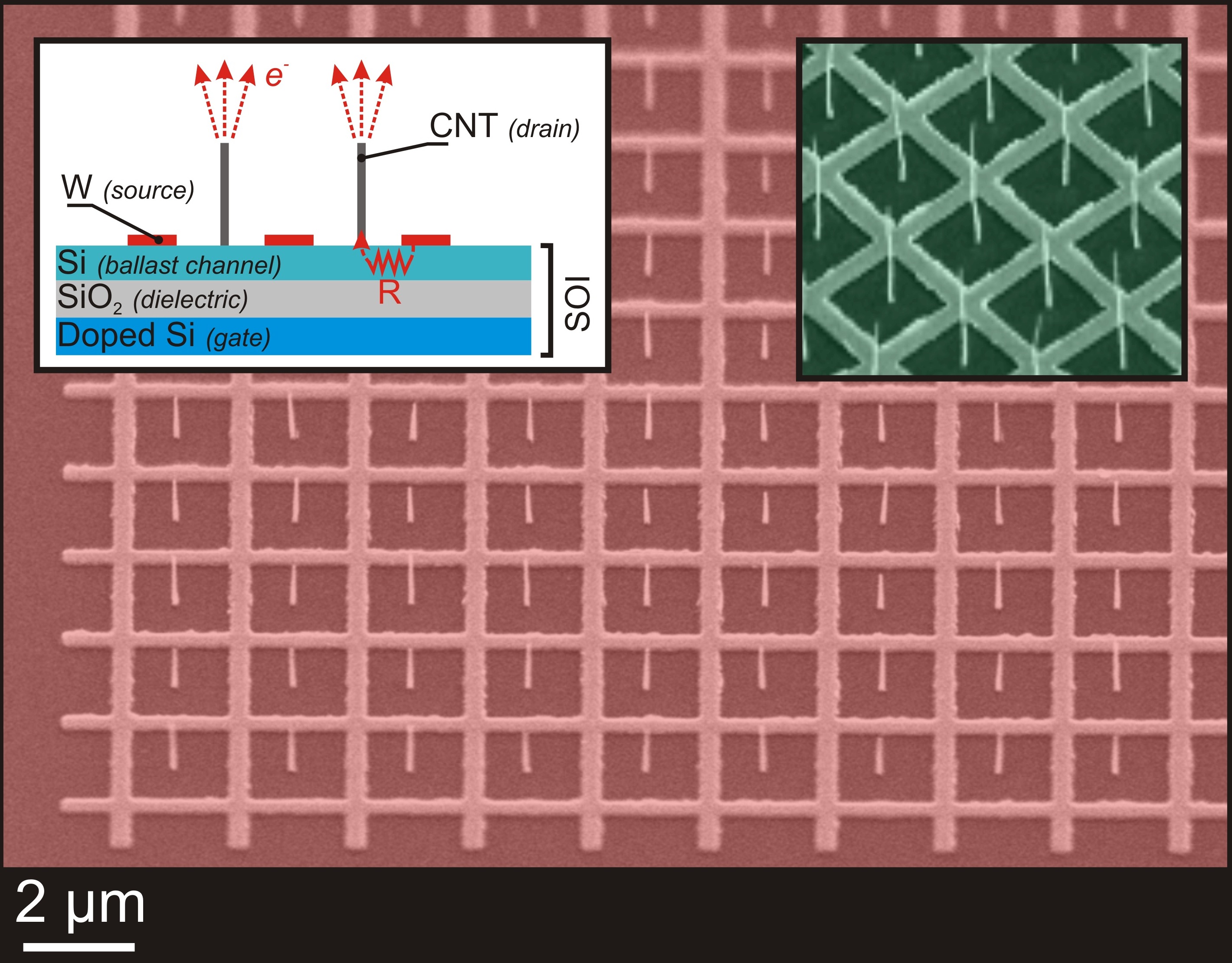
Here we develop novel nano-micro scale ballasting structures to prevent avalanche run-away and consequent destruction of the CNT emitters. I also investigate potential new nanocarbon triode structures based on graphene and CNTs, as well developing nanostructured field emission displays. CNTs are particularly resilient to bulk mobilisation making them temporally stable and particularly well suited for highly parallel electron lithography systems, travelling wave tubes, microwave amplifiers, displays, nanoscale vacuum power electronic devices, and X-ray sources.
-
Vacuum-based devices initiated modern day electronics, though were superseded by solid-state devices due to their potential for rapid miniaturisation. Global data usage is increasing rapidly. In the UK the average household has 7 internet connected devices. Our data consumption is increasing at a profound rate. The average home consumed some 35% more data in 2015 than in 2014. Our mobile communications data needs are increasing at a similarly high rate, with 78% of British adults accessing the internet each day in 2015, compared to just 35% in 2006. With Machine-to-Machine (M2M) communications becoming increasing common, estimates suggest that there are between 8-12 billion connected devices Worldwide, with predictions suggesting this may reach 100 billion by 2020. In 2017 there will be, on average, 1.7 connected devices for each and every person on the planet. We live in an ever increasingly connected world. The need for advanced high data rate communications devices are critical to support such astounding data growth and whose development will ultimately underpin the future global connectedness and Internet of Things (IoT).
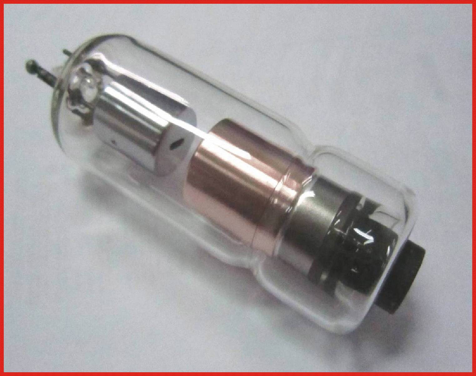
Though developed some six decades ago, electron emission based travelling wave tube amplifiers still dominate satellite communications with state-of-the-art devices operating at 200 W / 22 GHz, with efficiencies approaching 70 percent and rated lifetimes exceeding 15 years. In these power applications solid-state electronics have been found wanting due to their poor radiation resistance and deleterious functional shifts with the unavoidable increase in their operation temperature. Low voltage (< 10 V) solid-state devices require high operating currents to derive high output powers, which creates significant waste heat, with many parallel devices needed to produce a significant power output. Vacuum devices, on the other hand, operate at tens of thousands of volts, which when coupled to recent advances in compact high-voltage power supplies, only require a single low beam current to stimulate a high output power. Both cost and complexity can be reduced through the use of vacuum-based power electronics. Advances in materials science and ultra-precision engineering at the nanoscale are proving to be an essential component in developing emerging vacuum-based electron sources which offer a potential means to realise the next global high-data rate network through the development of ultra-compact and ultra-efficient cold-cathode travelling wave tubes.
Valves, thermionic electron emission vacuum tubes, were the central computational elements of the World's first computers; Colossus and ENIAC. The emergence of solid-state transistors in 1947, which could be aggressively miniaturised, coupled to the high failure rate of thermionic valves, resulted in the solid-state electronics era upon which our modern society pivots. Valves and vacuum computation devices are considered by many to be out-dated. However, the approaching fall of Moore's Law is stimulating the wider electronics community to embrace new device architectures with vacuum-gap devices offering one viable solution. Here we investigate the fabrication and functionality of highly parallel on-chip vacuum field emission nano-computation elements for high data rate computation by removing the channel-limiting transit times.
-
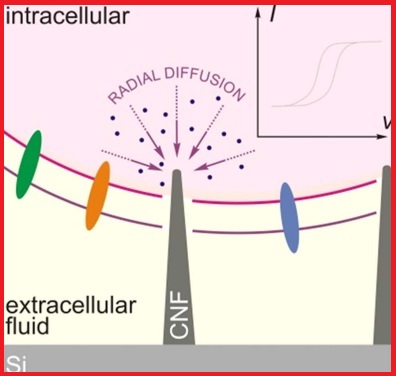
Bio-electronics and nanomaterials represent two research themes of recognised international strategic importance. Faced with a national increasingly aging population and huge international class inequalities in the provision of healthcare, new technology-driven approaches to the provision of monitoring, in-situ care, and data transmission via imperceptible e-plasters is urgently needed. Capitalising on the unique mechnical, optical and electrical properties of emerging nanomaterials, this research seeks to solve these pressing global challenges through the development of nanomaterial-based on-body biosensor and bioelectronics.
Sponsors