Schottky diodes are generally chosen for space-borne instrumentation, as their behaviour as non-linear heterodyne mixers and frequency multipliers is well understood and they can be operated without the need for cooling to low temperatures.
|
Schottky diodes are generally chosen for space-borne instrumentation, as their behaviour as non-linear heterodyne mixers and frequency multipliers is well understood and they can be operated without the need for cooling to low temperatures. |
|
| |
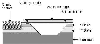
Good performance at millimetre wavelengths has been achieved with planar, air-bridged Schottky diodes. Performance is improved by reducing the parasitic capacitance of the structure by removing high permittivity GaAs from around the contact pads. The schematic on the left shows a cross-sectional view through a typical, air-bridged diode structure. |
|
The diode has a Pt/Au anode, formed on a GaAs substrate. Anodes are formed through via holes lithographically defined in a thin layer of SiO2 covering the GaAs. Gold contact pads are deposited on top of the SiO2 with a narrow finger making contact to the anode. A trench is etched underneath the finger, removing GaAs to reduce the parasitic capacitance of the device. |
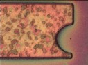 |
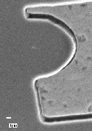
A key step in the fabrication process is the formation of the via hole through which the anodes are formed. The optical image on the left shows a resist window of 500nm diameter aligned to an ohmic contact pad. The resist window was formed using electron-beam lithography. The SEM image on the right shows the sample after reactive ion etching has transferred the 500nm diameter pattern to the silicon dioxide layer. |
 |
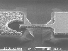 |
The SEM image on the left shows a complete, planar, air-bridged Schottky diode. For remote sensing applications, an anti-parallel diode configuration is often preferred. The optical image on the right shows an anti-parallel pair of diodes. |
 |
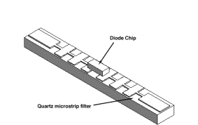
| Individual diode-pair chips of size 100 x 60 microns are diced from the GaAs wafer for mounting in waveguide mixer mounts. The diode chip is flip-chip soldered onto a metallised microstrip filter formed on a quartz substrate. The filter drops into a channel cut across the waveguide in which the device sits. |
 |
|
SRD 21 Jan 05