Applications
(i) Measurement of ion dose and uniformity
The primary motivation for the development of the bench-top tool was the requirement for metrology techniques capable of providing information on the dose and uniformity of ultra-low energy implants. We demonstrated the essentially universal PAS response to ion dose, for a large rage of ion masses and energies, at the beginning of the project. We have since demonstrated the ability of PAS to monitor dose variations as a function of wafer area and depth resulting from sub-keV and keV ion implantation . Recently, we have described the response of PAS to MeV ion implantation. The study analyzed response to ions varying in mass and energy from protons at 450keV, to Ge+ at 4MeV. The results led to the deduction of a relationship between ion dose (normalized using TRIM), (fA), and vacancy-type defect concentration, (C), at ĮRp such that
C= (2.79x10¹⁰)fA0.63 (1)
for all ions in the energy and dose range used in the study. In addition to being a straightforward and reliable expression for estimating aggregated, vacancy-type defect concentrations following MeV implantation, (1) implies the ability to determine implanted dose for a wide range of implantation conditions using only the raw PAS data and TRIM output.
PAS may be used with varying sensitivity to monitor implant dose from 1x10¹⁰ ¢ 1x1016cm-2 and implant energy from sub-keV to MeV. In many cases, the raw PAS data can be used to provide an absolute measure of dose within an accuracy of <10%.
The ability to probe depth-dependent defect distributions with a focused positron beam of ~ 1mm diameter also offers the opportunity to measure non-uniformities in the concentration of open-volume defects across a wafer. Such non-uniformities can be caused by many different phenomena, depending on the sample and the process undertaken.
The first scan by the compact beam of a 4" Si wafer centrally implanted with 120keV O ions is shown as a false-colour plot in the panel opposite.
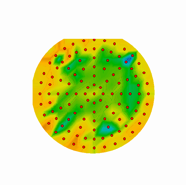
First whole-wafer scan; red dots indicate positron beam positions
(ii) SIMOX process control
Separation by implantation of oxygen (SIMOX) is a well-established technique for producing silicon-on-insulator (SOI) structures. Ion energies of 100-200keV at doses approaching 1018cm-2 are typical in the fabrication of conventional SIMOX, however much of the current research is aimed at developing low-dose fabrication processes where the implanted dose is at least one order of magnitude lower, with significant reduction in fabrication time and cost.
A significant disadvantage to the use of spectroscopic ellipsometry to measure ion dose is the requirement for the measured sample to be a fully formed SIMOX wafer, having undergone a post-implant high temperature anneal for several hours. PAS is known to be highly sensitive to the structure of silicon following high dose oxygen implantation; the S parameter versus energy curve typically has a peak (corresponding to voids generated near to the Si surface) followed by a valley (resulting from positron interaction with defects complexed with the end of range oxygen).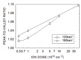
PAS peak-to-valley parameter vs ion dose for 120 and 190keV O+-implanted Si (as-implanted)
(iii) Monitoring of void formation
It has been known for some time that nanocavities can be formed by high-fluence implantation of H or He. Post-implantation annealing causes the implanted species to outgas leaving behind microscopic voids. This process has found use as an efficient method for forming gettering centres in Si. The implantation of H in particular is also an important step in the UNIBONDę process.
PAS is a particularly appropriate technique for monitoring the formation and evolution of vacancy clusters into small nanocavities. The graph shows S parameter values versus mean probed depth for He+-implanted Si (100keV, 5x1016cm-2), both pre- and post-thermal processing. The circles represent data for the as-implanted sample. Here the S parameter value of only 1.03 indicates the presence of small vacancy-type defects. The up-triangles are data taken from the same sample following a thermal annealing step. The increase of the S parameter to ~1.06 indicates the formation of a layer of small voids at a depth of ~500nm, consistent with the depth of peak disorder. The remaining data, taken from a sample with a small difference in processing history, indicate the presence of point defects co-existing with a layer of voids at the end-of¢range. The ability of PAS to monitor the different stages of void formation is clear.
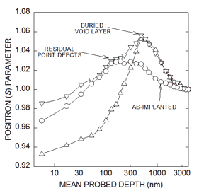
Raw PAS data for 100keV He+-implanted Si at 5x1016cm-2.
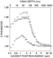
S vs positron energy for SiN films. O: 68% Si, 112nm film. É : 52% Si,
133nm film. D : 37% Si, 51nm film.
(iv) Characterisation of thin films
There exists in principle a unique S parameter value for each element of the periodic table; PAS can thus provide non-destructive information on the structure and stoichiometry of thin films. The adjacent figure shows S parameter vs incident positron energy for three PECVD-deposited SiN films of different Si composition. The films were characterized using Rutherford backscattering to determine the %Si values. The trend of decreasing S parameter with decreasing Si content can be easily calibrated. Although in this case ellipsometry would be the spectroscopy of choice, PAS can probe the composition of any film (of depths of several mm), including polymer and metallic layers. When used in conjunction with techniques such as ellipsometry, the density of thin films can readily be determined .
We have also demonstrated the effectiveness of beam-based PAS in the study of Ga vacancies and dislocations in GaN films grown by MOCVD and vacancies in MBE-grown SiGe layers.
Among the most promising of other potential applications are (a) the non-destructive monitoring of pore sizes in low-k films by measuring the positronium formation fraction: (b) the non-destructive measurement of p-n junction depths (eg, for 2-100keV B implantation of Si in the range 50-500nm, with a sensitivity of 10nm), and ¢ using the same technique ¢ identification of ion-implanted wafers which have been poisoned with higher energy implants.
(vi) Other relevant measurements
Development work on improving the PAS technique and thus the performance of the compact beam included a detailed consideration of the optimum sensitivity of the PAS parameter S and research on improving the efficiency of positron moderators. Finally, key work aimed at gaining new understanding of the formation, diffusion, trapping and precipitation of fluorine and oxygen in silicon was undertaken.
