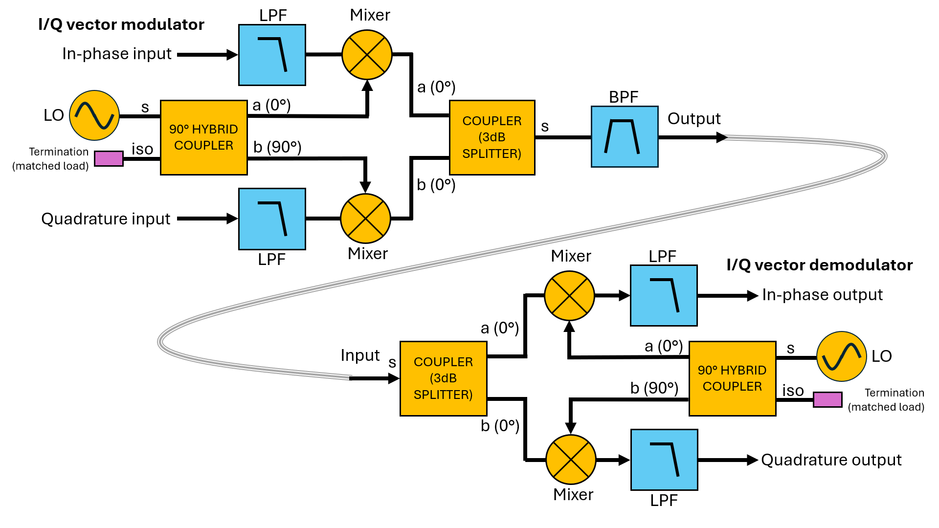
Demodulation using a vector demodulator
Vector demodulation experiments - introduction
In this second simulation-based lab experiment we will examine circuits for phase demodulation using a vector demodulator. This is also sometimes known as an I/Q or quadrature demodulator. This lab is less focussed on specific measurements and more about reinforcement of your understanding of vector modulation and demodulation. The main aim of this lab is to highlight the importance of both frequency and phase synchronization in the demodulation process, as well as reinforce your understanding of other topics such as inter-symbol interference and analogue filters. Finally, we look at complete end-to-end QPSK based communications system. These exercises will pose a number of questions for you to think about. The answers to these questions will be discussed after the lab session.
To make the process easier to understand, for these simulations we will begin with setting both the RF and the LO signals for our I/Q demodulator to the same frequency, at approximately 10 MHz. This means that at the IF outputs, the first order sum and difference mixer terms will be 0 MHz (i.e. DC) and 20 MHz. To ensure adequate suppression of the 20 MHz component at the IF output there is a low-pass filter. In this the configuration, the values of the DC components at the I and Q outputs are related to the phase difference between the RF input and the LO signal. This configuration is often referred to as a Zero-IF (ZIF or homodyne) architecture. We’ll revisit the various types of transceiver architectures in EE22006 later in the course.
The laboratory simulation exercises in this activity are:
- Low-pass filter responses and pulse dispersion measurement.
- I/Q demodulation for phase estimation.
- End-to-end simulation of a QPSK (Quadrature Phase-Shift Keyed) communications link.
Low pass filter responses
We will examine the characteristics of three different low-pass filters that could be used in the IF output of our I/Q demodulator. Each filter has nominally the same -3dB bandwidth, but with slightly different magnitude and phase responses as we shall see. Load the EE22005_LPF_transient_ChebButtElip.asc file into LTspice and study the schematic carefully. You will observe that we have three filters each driven by the same ideal voltage source but via their own separate source impedance. This enables us to excite all three filters simultaneously but without any interaction between them. As with all these experiments, the input, output and characteristic impedances are $Z_S,Z_L,Z_0=50$ Ω. We’ve already seen that we can determine the frequency response of such circuits using a small-signal AC simulation (via the .ac simulation command). However, here we will use transient simulation. We will excite the filter with a short pulse, and then by Fourier transforming the time domain results, examine the frequency response. Recall that an ideal Dirac impulse (infinitesimal pulse width) has a spectrum that is constant across all frequencies. A true Dirac pulse obviously isn’t realisable so we will use a very short 30 ns pulse which still has a very wide “sinc( )” response in the frequency domain, that extends beyond the passband of the filter. If we excite the filter with such a suitably narrow pulse, the filter output will contain all frequency components falling within its pass band. Also included in the circuit here is a transmission line element which adds a small delay. This enables us to separate the input and output pulses in time to make them more visible.
Impulse response
Now let’s characterise the filter based on its response to a single short pulse:
- Run the simulation and plot only the three output waveforms: out_b, out_c, and out_e.
- Measure the width of the first positive going part of the output waveform at approximately 1.6 µs. Measure the width of the output at the points the waveform is half its positive peak value. An easy way to do this is with the cursors (type “c” in the plot window). Use one cursor to find the peak. Use a second cursor to move to one-half the voltage value to the right of the peak, then move the first cursor to the point left of the peak at the same voltage. The difference between the two cursor times gives the width.
- Record the output widths for all three outputs.
- Change the width of the input excitation pulse to 300 ns, re-run the simulation record the output pulse widths.
- Why is the output pulse so much wider than the input when the 30 ns input pulse is used? Why is this not the case for the 300 ns pulse?
Frequency response
Now let us look at the frequency responses of the three filters. From signal theory we know that the frequency response of a linear time-invariant system is the Fourier transform of its impulse response.
- First, return the pulse width of the excitation source to 30 ns. Re-run the simulation and now add the input signals (in_b, in_c, in_e) to the simulation output plots. We note that in addition to the input pulse at a time of 0.4 µs, there is also something appearing at the input at 2.4 µs.
- To explain and understand what this additional part of the waveform is, let’s look at the Fourier transform of these waveforms. Right-click in the plot window and select View->FFT. In the pop-up window, select the “Specify a time range” radio button. This will allow us to compute the FFT of a subset of the simulated data. To exclude the excitation pulse on the input waveforms set the start time of the FFT to 0.8 µs. Plot the Fourier transforms of all the waveforms and observe the results.
- Measure the approximate -3 dB bandwidth of each of the three outputs (out_b, out_c, out_e). Also determine the -60 dB bandwidth. You might find it easier to plot one filter output at a time to do this.
- Now consider the FFTs of the input waveforms (in_b, in_c, in_e). Can you explain the frequency content of this waveform? Hint: why does the amplitude appear to be much less in the low-pass filter passband region and much higher beyond the low-pass filter’s cut-off frequency?
I/Q demodulator
Let us now consider the I/Q vector demodulator. Load and study the schematic file EE22005_vectordemod.asc. Note how similar it looks to the previously considered vector modulator. In effect the circuit is identical, it’s almost just flipped left-to-right. In this case the input is the RF side of the mixer, and the outputs are the I and Q IF signals. Note that at the I and Q IF outputs this circuit uses Butterworth response low-pass filters like the ones we’ve just looked at.
Basic operation
To characterise this circuit, we only need a short transient (time domain) simulation. We can also skip the initial start-up transient response which is less than 1 µs. We can do this by setting the simulation command to .tran 2u 1u. We can now examine the response.
- Run the simulation. Plot out the if_dn_i and if_dn_q signal traces. Observe that these are more or less constant DC values over the 1 µs with minimal variation. If the RF and LO frequencies are identical the I/Q IF outputs are DC voltages related to the phase.
- Now let’s configure LTspice to make automatic measurements of the time averages of these waveforms. Remember to add a simulation directive we click the “.t” icon on the top menu bar. To measure the average waveform values, add the following directives to the simulation schematic: .meas TRAN v_inphase AVG V(if_dn_i) .meas TRAN v_quad AVG V(if_dn_q) This will generate two measurements named v_inphase and v_quad which are the arithmetic means of the waveforms over the simulation period. In our case it will be the 1 µs period we’ve set the simulation to run for.
- Run the simulation again and confirm that the average values reported in the LTspice log (obtained by typing Ctrl+L) agree with what you see in the plots.
I/Q demodulation
To demonstrate the ability of the I/Q demodulator to measure phase we need to offset the phase difference between the RF input and the LO signal. We will again use the EE22005_vectordemod.asc file. By varying the phase difference between these two signals, we can observe what happens to the I/Q voltages at the IF outputs. We could do this by changing the phase of the RF source manually. This sounds a little tedious. So instead, let’s use the .step directive and let LTspice run a series of simulations automatically.
- Right click on the RF input source. In the time-domain source settings, set the phase term “Phi[deg]” to be a variable rather than just a value. We can do this by setting the value to “{phi}”. The curly brackets { } let LTspice know that the named variable is a parameter whose values we’ll define elsewhere. We can then define different values for phi using the .step directive. Add a new LTspice directive and set it to the following: .step param phi -180 180 10 When the simulation next runs, LTspice will sequentially set the value of phi from -180° to +180° in steps of 10° degrees. LTspice will run a separate simulation for each value. As it does so it will also record the average values of the I and Q signals as v_inphase and v_quad in the LTspice log file.
- With these directives set, re-run the simulation. In the plot window observe that for the different phases that the I and Q outputs change but are within similar maximum and minimum values. However, it’s a little difficult to see what’s happening, so let’s look at a different way of representing the I and Q outputs.
- Bring up the LTspice log (Ctrl+L). Now right-click in this log window and select the option of “Plot .step’ed .meas data”. This will bring up a new plotting window. The abscissa (x-axis) is currently labelled with the values of the .step parameter “Phi”, from -180° to +180°. Either type “a” in this window or right-click and select “Add Traces”. This will bring up a new window titled “Add Traces to Plot”, select both v_inphase and v_quad from the list and click OK.
- Observe the results. Is this what you’d expect to see? Use the cursors (type “c” in the window) to measure the phase when the I and Q traces have values of 0 Volts. At a phase shift of 0° why do you think the values of I and Q not zero?
- To try and understand what’s going on, let’s plot I against Q. Delete the v_inphase form the plot window, leaving only the v_quad trace. Now right click on the x-axis to bring up a dialog box. Change the “Quantity Plotted:” box to v_quad. To make it easier to understand resize the plot window so it’s approximately square. Let’s also make the data points more visible. Right click in the window and navigate the pop-up menu to View->Mark Data Points. Observe the results, is this what you’d expect to see?
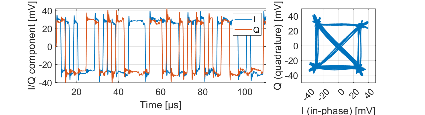
- For the next step, let’s again make it little easier to see what’s happening by reducing the number of phase values. In the .step command for phi, make the increment 90°. Re-run the simulation and replot I (v_inphase) against Q (v_quad). Now look at the position of the data points - in effect this plot is the constellation plot for a QPSK (Quadrature Phase-Shift-Keyed) signal.
Transmission line delay
To help understand why the constellation might not look as you expect, let’s now also step a second parameter, the delay of the transmission line. Right click on the transmission line component. Change the fixed value of the delay Td to be a parameter, by making changing “Td=10n Z0=50” to be “Td={tau} Z0=50”. Now add another .step command for to vary this delay: .step param tau 10e-9 90e-9 10e-9 Re-run the simulations, and replot I against Q. Observe what happens as the delay varies. What does this suggest is necessary for demodulation of QPSK and QAM signals at the receiver?
End-to-end vector modulation and demodulation
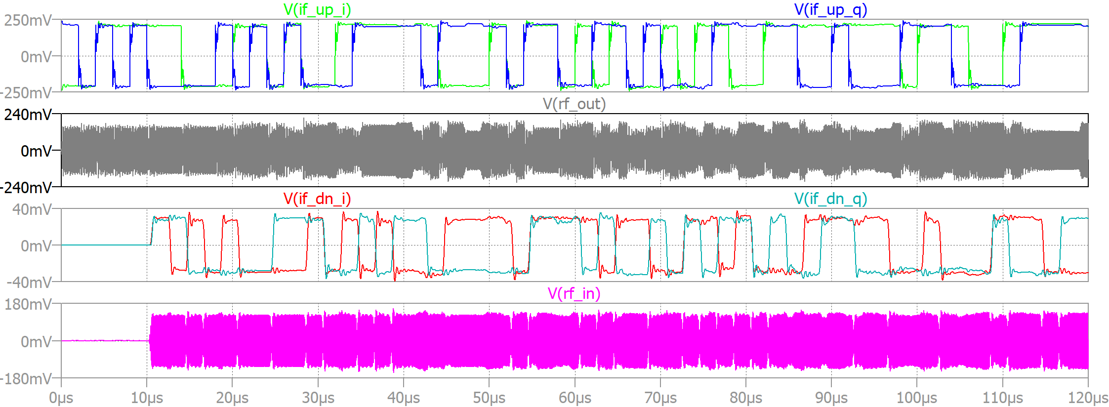
Having considered vector modulation and demodulation separately, let us now look at an end-to-end system. Load the schematic EE22005_updown_vectormod.asc. Most of the circuit should by now look quite familiar. There are few changes, however. If you look at the IF I and Q inputs to the modulator, if_up_i and if_up_q, you will see they are driven from “behavioural sources” B1 and B2. If you right mouse click on one of them, you will see that the value of the source is complicated looking function. This generates a random sequence of binary symbols and maps them to a value that is $\pm$ 300 mV. The two sources B1 and B2 are configured slightly differently so that they generate two fairly random sequence of bits that can be sent over our QPSK link (if you want to explore how this works on its own, open and the run the EE22005_basebandgen.asc and plot the I and Q signals).
Activities:
- Run the simulation for EE22005_updown_vectormod.asc,
- Examine the I and Q waveforms at the input and the output of the demodulator (the signals labelled if_up_i, if_up_q and if_dn_i, if_dn_q). You should see something similar to that shown in the figure.
- You might find it helpful to plot the modulator and demodulator signals in different plot panes as shown in the figure above (right click in the plot window, you should see an option to “Add Plot Pane Above”, “Add Plot Pane Below” plus some other options, it might take some experimentation to familiarise yourself with all how it works).
- Note that, aside from a delay and being of different amplitude, the I/Q symbols at the input and the output are identical. However, in this instance I’ve pre-adjusted the transmission line delay to 10.045 µs to closely align the I/Q symbols.
- We know that the period of the 10 MHz RF carrier is 100 ns. That is, every 100 ns of delay in the transmission line corresponds to exactly 360° change in phase. Investigate what happens to the I and Q values either the delay or phase of the demodulator LO source (V6) changes. What would happen if you have either a phase shift or delay equivalent to 90° ?
Final comments
This is the end of the structured activities of this lab. There is lots more to explore but you’re welcome to stop here. Hopefully you will have learned something about LTspice which will prove useful throughout the rest of your degree, but also it will helped cement your understanding of I/Q modulation, and some of the challenges of communications engineering. A final note about the circuits. The performance of this modulator is not the best. There are no active (amplifier) devices. This means that signals can easily “leak” or “couple” to other parts of the circuit where we don’t necessarily want them to. For example, in the first lab when you looked at the mixer you probably saw that although we label the ports LO, RF and IF. When you looked at the spectra at any of the ports, all the other signals were also present, albeit at perhaps a smaller amplitude. For example, if you look at the IF signal you can likely see frequency components due to the LO signal and the RF signal– which ideally wouldn’t be there. There is a lot we can do to improve performance as you’ll see in later years and commercially produced mixers, modulators and integrated circuits are capable of much better performance. However, even the very best devices will still exhibit some of the behaviours that you’ve seen first hand in this lab.
Feel like an extra challenge?
It’s possible to run LTspice from a command line without the GUI, in a so-called batch mode. Even better, we can actually run it via other tools such as MATLAB, and then use MATLAB to read and plot the data for further analysis. This can be used as a convenient way of running a lot of simulations without need for any user interaction. I’ve created a separate zip file for this to get you started (EE22005_matlab.zip). The main script is EE22005_runsim.m. This calls LTspice twice, first to generate the netlist and then again to run the actual simulation (you might need to adjust the paths to the executables). It requires an additional function which is included to read-in an ASCII version of the LTspice output file (link here: https://github.com/PeterFeicht/ltspice2matlab). In order to reduce the data that LTspice generates you will notice an extra .save directive in the schematic, this limits the output file contents to only named nodes. When you run the MATLAB script it will run the LTspice simulation and then generate a plot of the I/Q time-series which will produce a figure that looks something like this.
What now? This is up to you! One thing you could do is write a function to calculate Error Vector Magnitude (see the EE22006 lecture on non-linearity). There are countless other options, you could try. If you prefer, there are also libraries and tools to drive LTspice within a Python environment e.g., https://pypi.org/project/PyLTSpice/