Lab 1 - Designing In OrCAD [Part 2/3]
Designing in OrCAD Version 17.4.
Page 2 of 3.
Physical Layout
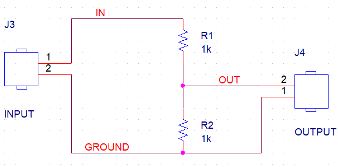
Before we start creating our PCB Layout based on this schematic design, we first need to make a few changes to the schematic. For any circuit that will ultimately be connected to another external circuit we must ensure there is a means of connecting the two circuits together. This is achieved by adding connectors or jacks. Let’s add the connectors as shown in .
To add the connectors use the Place>Part command (or the P shortcut), add the “CONNECTOR” library by navigating up one level in the root directory and then locate the CON2 part and place it twice, as shown in . These are the input and output headers. You may need to use right-click>Mirror Horizontally or Vertically or the right-click>Rotate command to get the orientation to match the schematic. Change the name of the connector (by double clicking in CON2 text) to INPUT and OUTPUT in the Value field in the Display Properties box. Delete all voltage sources and grounds and using the W shortcut, ensure you wire up your input and output headers as shown in .
A collection of joined wires in a circuit is called a Net. In complex circuits there can be very large numbers of nets. Nets can be given a name (an alias) and using aliases can make the design process much easier. To do this click Place>Net Alias (or use the N shortcut). In the “Place Net Alias” popup window, in the Alias field type IN and click OK. Click on the wire that is to form the IN net, as shown in . Press ESC to end the net alias placement process or the right-click>End Mode command. Repeat this process to assign the GROUND and OUTPUT net aliases to the wires, as shown in . Your circuit should now look like .
The schematic so far only includes component symbols that allow us to analyse the circuits functionality, however the design does not yet have any details on the actual physical dimensions and geometries for these components. Of course, in order to design the final PCB layout it is essential such information is included in the design. We will do this next.
To do this we assign each component with a footprint. Footprints depict the physical pin positions and sizes of the actual device. It is important the correct footprints are used otherwise the manufactured PCB may be incorrectly designed and may not be able to mount the desired component. Footprints are largely standardised for many components, but for more esoteric devices their footprints can also be downloaded directly from the component supplier or manufacturer. This can save designers a great deal of time.
For our design, we next need to assign the PCB footprint property values for all the parts in the design. You will need to specify the PCB Footprint property values for the names of the footprints that match the footprints in your libraries. Typically, in your Cadence folder, e.g.:
C:\Cadence\SPB\_17.4\share\pcb\pcb\_lib\symbolsyou will find the existent footprints for your designs. Please note that this folder path may change depending on the exact specifications and type of computer you are using.
Other than using standard footprints or importing new footprints directly from the manufacturers, it is also possible to create your own if required. Should you require a footprint that is non-standard and that has not been provided by the supplier, SnapEDA is a commonly used webpage from which you can download missing PCB footprints. In our present design we will be using footprints that have already been made available to use in the software. Footprints have the file extension .dra. Note that there will need to be an exact match between the numbered pins in the schematic part and the numbered pins on the PCB Footprint.
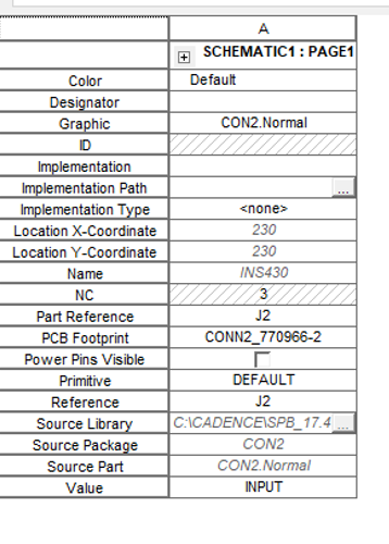
One possible method to add footprints to your schematic components is described in this section. Let us add a footprint for one of the connectors. Select the INPUT header and right-click>Edit Properties… to launch the Property Editor. (You can also double-click on the part to bring up the Property Editor). It is often easier to use the spreadsheet in the Property Editor window by transposing it. To do this double click in the top left cell. The value in the “PCB Footprint” field defines the file called for the parts footprint. Ensure that all the cells have the same content as shown in . When you are finished, save the changes (File > Save💾) and close the Property Editor. Repeat the steps for the OUT header.
Design Rule Checks
Creating a Netlist
Problems with PCB Editor Crashing – Potential Fixes
Setting up PCB Editor
Creating a Board Outline
Changing Layout Colors
Adding Mounting Holes
Placing Components.
Design Rule Checking
Setting the Design Constraints
Routing
Manual Routing
Adding Vias and Layers Whilst Routing.
Checking & Reviewing
Back Annotation (*optional)
Page 2 of 3.